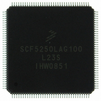
SCF5250LAG100 Freescale Semiconductor, SCF5250LAG100 Datasheet - Page 18

SCF5250LAG100
Manufacturer Part Number
SCF5250LAG100
Description
IC MPU COLDFIRE 100MHZ 144-LQFP
Manufacturer
Freescale Semiconductor
Series
SCF52xxr
Datasheet
1.SCFLXRAYADPTS12.pdf
(56 pages)
Specifications of SCF5250LAG100
Core Processor
Coldfire V2
Core Size
32-Bit
Speed
100MHz
Connectivity
EBI/EMI, I²C, IDE, MMC, SPI, UART/USART
Peripherals
DMA, I²S, POR, Serial Audio, WDT
Number Of I /o
57
Program Memory Type
ROMless
Ram Size
128K x 8
Voltage - Supply (vcc/vdd)
1.08 V ~ 1.32 V
Data Converters
A/D 6x12b
Oscillator Type
Internal
Operating Temperature
-20°C ~ 70°C
Package / Case
144-LQFP
Eeprom Size
-
Program Memory Size
-
Available stocks
Company
Part Number
Manufacturer
Quantity
Price
Company:
Part Number:
SCF5250LAG100
Manufacturer:
Intersil
Quantity:
90
Company:
Part Number:
SCF5250LAG100
Manufacturer:
Freescale Semiconductor
Quantity:
10 000
Part Number:
SCF5250LAG100
Manufacturer:
FREESCALE
Quantity:
20 000
3.15
The QSPI interface is a high-speed serial interface allowing transmit and receive of serial data. Pin
descriptions are given in
3.16
The XTRIM/GPIO0 output produces a pulse-density modulated phase/frequency difference signal to be
used after low-pass filtering to control varicap-voltage to control crystal oscillation frequency. This will
lock the crystal to the incoming digital audio signal.
3.17
The MCLK1/GPIO11 and QSPI_CS2/MCLK2/GPIO24 can serve as DAC clock outputs. When
programmed as DAC clock outputs, these signals are directly derived from the crystal oscillator or clock
Input (CRIN).
18
DDATAO/CTS1/SDATA0_SDIO1/GPIO1 Secure Digital serial data bit 0
RCK/QSPI_DIN/QSPI_DOUT/GPIO26
RCK/QSPIDIN/QSPI_DOUT/GPIO26 Multiplexed signal IIC interface data or QSPI data input. Function select is done via
DDATA1/RTS1/SDATA2_BS2/GPIO2
QSPICS1/EBUOUT2/GPIO16
QSPI_DOUT/SFSY/GPIO27
SCL0/SDATA1_BS1/GPIO41
QSPICS0/EBUIN4GPIO15
QSPICS2/MCLK2/GPIO24
QSPICLK/SUBR/GPIO25
CS1/QSPICS3/GPIO28
SDA0/SDATA3/GPIO42
Flash Memory Signal
Serial Module Signal
Queued Serial Peripheral Interface (QSPI)
Crystal Trim
Clock Out
Table 11. Queued Serial Peripheral Interface (QSPI) Signals
Table
Table 10. Flash Memory Card Signals (continued)
11.
SCF5250 Data Sheet:
Multiplexed signal IIC interface clock or QSPI clock output Function select is done via
PLLCR register.
PLLCR register.
QSPI data output.
4 different QSPI chip selects.
Memory Stick interface 1 data I/O
Secure Digital serial data bit 1
Memory Stick interface 1 strobe
Secure Digital serial data bit 2
Memory Stick interface 2 strobe
Reset output signal
Selection between Reset function and SDATA2_BS2 is done by programming PLLCR
register.
Secure Digital serial data bit 3
Technical
Data,
Description
Description
Rev. 1.3
Freescale Semiconductor


