SCF5250LAG100 Freescale Semiconductor, SCF5250LAG100 Datasheet - Page 4
SCF5250LAG100
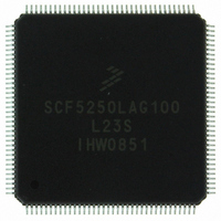
Manufacturer Part Number
SCF5250LAG100
Description
IC MPU COLDFIRE 100MHZ 144-LQFP
Manufacturer
Freescale Semiconductor
Series
SCF52xxr
Datasheet
1.SCFLXRAYADPTS12.pdf
(56 pages)
Specifications of SCF5250LAG100
Core Processor
Coldfire V2
Core Size
32-Bit
Speed
100MHz
Connectivity
EBI/EMI, I²C, IDE, MMC, SPI, UART/USART
Peripherals
DMA, I²S, POR, Serial Audio, WDT
Number Of I /o
57
Program Memory Type
ROMless
Ram Size
128K x 8
Voltage - Supply (vcc/vdd)
1.08 V ~ 1.32 V
Data Converters
A/D 6x12b
Oscillator Type
Internal
Operating Temperature
-20°C ~ 70°C
Package / Case
144-LQFP
Eeprom Size
-
Program Memory Size
-
Available stocks
Company
Part Number
Manufacturer
Quantity
Price
Company:

Part Number:
SCF5250LAG100
Manufacturer:
Intersil
Quantity:
90
Company:
Part Number:
SCF5250LAG100
Manufacturer:
Freescale Semiconductor
Quantity:
10 000
Part Number:
SCF5250LAG100
Manufacturer:
FREESCALE
Quantity:
20 000


1.2.7
The SCF5250 provides a glueless interface to 16-bit port size SRAM, ROM, and peripheral devices with
independent programmable control of the assertion and negation of chip-select and write-enable signals.
The SCF5250 also supports bursting ROMs.
1.2.8
The bus interface controller transfers information between the ColdFire core or DMA and memory,
peripherals, or other devices on the external bus. The external bus interface provides 23 bits of address bus
space, a 16-bit data bus, Output Enable, and Read/Write signals. This interface implements an extended
synchronous protocol that supports bursting operations.
1.2.9
The SC5250 digital audio interface provides three serial Philips IIS/Sony EIAJ interfaces. One interface
is a 4-pin (1 bit clock, 1 word clock, 1 data in, 1 data out), the other two interfaces are 3-pin (1 bit clock,
1 word clock, 1 data in or out). The serial interfaces have no limit on minimum sampling frequency.
Maximum sampling frequency is determined by maximum frequency on bit clock input. This is 1/3 the
frequency of the internal system clock.
1.2.10
The SCF5250 has one digital audio input interface, and one digital audio output interface. The single
output carries the consumer “c” channel.
1.2.11
The audio interfaces connect to an internal bus that carries all audio data. Each receiver places its received
data on the audio bus and each transmitter takes data from the audio bus for transmission. Each transmitter
has a source select register.
In addition to the audio interfaces, there are six CPU accessible registers connected to the audio bus. Three
of these registers allow data reads from the audio bus and allow selection of the audio source. The other
three register provide a write path to the audio bus and can be selected by transmitters as the audio source.
Through these registers, the CPU has access to the audio samples for processing.
Audio can be routed from a receiver to a transmitter without the data being processed by the core so the
audio bus can be used as a digital audio data switch. The audio bus can also be used for audio format
conversion.
1.2.12
The SCF5250 is capable of processing CD-ROM sectors in hardware. Processing is compliant with
CD-ROM and CD-ROM XA standards.
4
System Interface
External Bus Interface
Serial Audio Interfaces
IEC958 Digital Audio Interfaces
Audio Bus
CD-ROM Encoder/Decoder
SCF5250 Data Sheet:
Technical
Data,
Rev. 1.3
Freescale Semiconductor
Related parts for SCF5250LAG100
Image
Part Number
Description
Manufacturer
Datasheet
Request
R

Part Number:
Description:
Scf5250 Integrated Coldfire Microprocessor Data Sheet
Manufacturer:
Freescale Semiconductor, Inc
Datasheet:
Part Number:
Description:
Manufacturer:
Freescale Semiconductor, Inc
Datasheet:
Part Number:
Description:
Manufacturer:
Freescale Semiconductor, Inc
Datasheet:
Part Number:
Description:
Manufacturer:
Freescale Semiconductor, Inc
Datasheet:
Part Number:
Description:
Manufacturer:
Freescale Semiconductor, Inc
Datasheet:
Part Number:
Description:
Manufacturer:
Freescale Semiconductor, Inc
Datasheet:
Part Number:
Description:
Manufacturer:
Freescale Semiconductor, Inc
Datasheet:
Part Number:
Description:
Manufacturer:
Freescale Semiconductor, Inc
Datasheet:
Part Number:
Description:
Manufacturer:
Freescale Semiconductor, Inc
Datasheet:
Part Number:
Description:
Manufacturer:
Freescale Semiconductor, Inc
Datasheet:
Part Number:
Description:
Manufacturer:
Freescale Semiconductor, Inc
Datasheet:
Part Number:
Description:
Manufacturer:
Freescale Semiconductor, Inc
Datasheet:
Part Number:
Description:
Manufacturer:
Freescale Semiconductor, Inc
Datasheet:
Part Number:
Description:
Manufacturer:
Freescale Semiconductor, Inc
Datasheet:
Part Number:
Description:
Manufacturer:
Freescale Semiconductor, Inc
Datasheet: