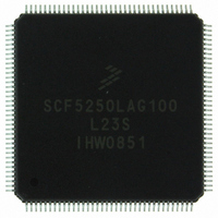
SCF5250LAG100 Freescale Semiconductor, SCF5250LAG100 Datasheet - Page 19

SCF5250LAG100
Manufacturer Part Number
SCF5250LAG100
Description
IC MPU COLDFIRE 100MHZ 144-LQFP
Manufacturer
Freescale Semiconductor
Series
SCF52xxr
Datasheet
1.SCFLXRAYADPTS12.pdf
(56 pages)
Specifications of SCF5250LAG100
Core Processor
Coldfire V2
Core Size
32-Bit
Speed
100MHz
Connectivity
EBI/EMI, I²C, IDE, MMC, SPI, UART/USART
Peripherals
DMA, I²S, POR, Serial Audio, WDT
Number Of I /o
57
Program Memory Type
ROMless
Ram Size
128K x 8
Voltage - Supply (vcc/vdd)
1.08 V ~ 1.32 V
Data Converters
A/D 6x12b
Oscillator Type
Internal
Operating Temperature
-20°C ~ 70°C
Package / Case
144-LQFP
Eeprom Size
-
Program Memory Size
-
Available stocks
Company
Part Number
Manufacturer
Quantity
Price
Company:
Part Number:
SCF5250LAG100
Manufacturer:
Intersil
Quantity:
90
Company:
Part Number:
SCF5250LAG100
Manufacturer:
Freescale Semiconductor
Quantity:
10 000
Part Number:
SCF5250LAG100
Manufacturer:
FREESCALE
Quantity:
20 000
3.18
These signals interface with external I/O to provide processor debug and status signals.
3.18.1
The TEST[2:0] inputs are used for various manufacturing and debug tests. For normal mode TEST [2:1]
should be ways be tied low. TEST0 should be set high for BDM debug mode and set low for JTAG mode.
3.18.2
The assertion of HI_Z will force all output drivers to a high-impedance state. The timing on HI_Z is
independent of the clock.
3.18.3
The internal PLL generates this PSTCLK/GPIO51 and output signal, and is the processor clock output that
is used as the timing reference for the Debug bus timing (DDATA[3:0] and PST[3:0]). The
PSTCLK/GPIO51 is at the same frequency as the core processor.
3.18.4
The debug data pins, DDATA0/CTS1/SDATA0_SDIO1/GPIO1, DDATA1/RTS1/SDATA2_BS2/GPIO2,
DDATA2/CTS0/GPIO3, and DDATA3/RTS0/GPIO4, are four bits wide. This nibble-wide bus displays
captured processor data and break-point status.
3.18.5
The processor status pins, PST0/GPIO50, PST1/GPIO49, PST2/INTMON/GPIO48, and
PST3/INTMON/GPIO47, indicate the SCF5250 processor status. During debug mode, the timing is
synchronous with the processor clock (PSTCLK) and the status is not related to the current bus transfer.
Table 12
Freescale Semiconductor
shows the encodings of these signals.
Debug and Test Signals
Test Mode
High Impedance
Processor Clock Output
Debug Data
Processor Status
JTAG operation will override the HI_Z pin.
SCF5250 Data Sheet:
NOTE
Technical
Data,
Rev. 1.3
19


