M30280FAHP#U5B Renesas Electronics America, M30280FAHP#U5B Datasheet - Page 217
M30280FAHP#U5B
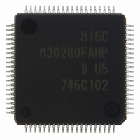
Manufacturer Part Number
M30280FAHP#U5B
Description
IC M16C/28 MCU FLASH 96K 80LQFP
Manufacturer
Renesas Electronics America
Series
M16C™ M16C/Tiny/28r
Specifications of M30280FAHP#U5B
Core Size
16-Bit
Program Memory Size
96KB (96K x 8)
Core Processor
M16C/60
Speed
20MHz
Connectivity
I²C, IEBus, SIO, UART/USART
Peripherals
DMA, POR, PWM, Voltage Detect, WDT
Number Of I /o
71
Program Memory Type
FLASH
Ram Size
8K x 8
Voltage - Supply (vcc/vdd)
2.7 V ~ 5.5 V
Data Converters
A/D 24x10b
Oscillator Type
Internal
Operating Temperature
-20°C ~ 85°C
Package / Case
80-LQFP
Controller Family/series
M16C
No. Of I/o's
71
Ram Memory Size
8KB
Cpu Speed
20MHz
No. Of Timers
10
Digital Ic Case Style
LQFP
Embedded Interface Type
I2C, UART
Rohs Compliant
Yes
Lead Free Status / RoHS Status
Lead free / RoHS Compliant
For Use With
R0K330290S000BE - KIT EVAL STARTER FOR M16C/29M30290T2-CPE - EMULATOR COMPACT M16C/26A/28/29M30290T2-CPE-HP - EMULATOR COMPACT FOR M16C/TINY
Eeprom Size
-
Lead Free Status / RoHS Status
Lead free / RoHS Compliant, Lead free / RoHS Compliant
Available stocks
Company
Part Number
Manufacturer
Quantity
Price


M
R
R
1
e
E
. v
6
Table 14.13 I
UART2 transmission
output delay
NOTES:
Factor of interrupt number
10
Functions of P7
Initial and end values of
SCL
J
Factor of interrupt number
15
Factor of interrupt number
16
Timing for transferring data
from the UART reception
shift register to the U2RB
register
Functions of P7
Functions of P7
Read RxD2 and SCL
levels
Initial value of TxD2 and
SDA
DMA1 factor (Refer to Fig.
14.23)
Store received data
Read received data
Noise filter width
0
C
2
9
(1)
(1)
(1)
1. If the source or cause of any interrupt is changed, the IR bit in the interrupt control register for the changed interrupt
2. Set the initial value of SDA
3. Second data transfer to U2RB register (Rising edge of SCL
4. First data transfer to U2RB register (Falling edge of SCL
2 /
0 .
B
2
2
(Refer to Fig.14.23)
8
(Refer to Fig.14.23)
(Refer to Fig.14.23)
0
may inadvertently be set to "1" (interrupt requested). (Refer to “Notes on interrupts” in Precautions.)
If one of the bits shown below is changed, the interrupt source, the interrupt timing, etc. change. Therefore,
always be sure to clear the IR bit to "0" (interrupt not requested) after changing those bits
disabled).
0
outputs
0
G
Function
4
SMD2–the SMD0 bits in the U2MR register, the IICM bit in the U2SMR register,
the IICM2 bit in the U2SMR2 register, the CKPH bit in the U2SMR3 register
J
7
a
o r
0 -
. n
u
2
p
3
0
0
1
2
, 1
0
(
pin
pin
pin
2
M
C bus Mode Functions
2
1
0
2
0
6
pin
7
C
2 /
CKPOL = 0 (rising edge)
CKPOL = 1 (falling edge)
Not delayed
RxD2 input
1st to 8th bits are stored in
the bit 7 to bit 0 in the U2RB
register
, 8
Clock synchronous serial I/O
mode (SMD2 to SMD0 = 001
IICM = 0)
UART2 transmission
Transmission started or
completed (selected by U2IRS)
UART2 reception
When 8th bit received
CKPOL = 0 (rising edge)
CKPOL = 1 (falling edge)
TxD2 output
15 ns
Possible when the
corresponding port direction bit
= 0
UART2 reception
U2RB register status is read
directly as is
page 195
CLK2 input or output selected
CKPOL = 0 (H)
CKPOL = 1 (L)
M
1
6
2
C
output while the SMD2 to SMD0 bits in the U2MR register is set to "000
2 /
f o
8
3
) B
8
5
2
,
CKPH = 0
(No clock delay)
Start condition detection or stop condition detection
(Refer to Table 14.14)
No acknowledgment
detection (NACK)
Rising edge of SCL
Acknowledgment detection
(ACK)
Rising edge of SCL
Delayed
The value set in the port register before setting I
(NACK/ACK interrupt)
Rising edge of SCL
SDA
SCL
Always possible no matter how the corresponding port direction bit is set
H
Acknowledgment detection
(ACK)
200 n s
1st to 8th bits are stored in
the bit 7 to bit 0 in the U2RB
register
I
IICM2 = 0
2
C bus mode (SMD2 to SMD0 = 010
2
2
input/output
input/output
2
9th bit)
(Cannot be used in I
2
9th bit)
(Clock delay)
CKPH = 1
L
2
2
2
9th bit
9th bit
9th bit
.
UART2 transmission
Rising edge of
SCL
2
C bus mode)
1st to 7th bits are stored into the bit 6 to
bit 0 in the U2RB register, with 8th bit
stored in the bit 8 in the U2RB register
UART2 reception
Falling edge of SCL
IICM2 = 1
(UART transmit/ receive interrupt)
CKPH = 0
(No clock delay)
UART2 transmission
Falling edge of SCL
Falling edge of
SCL
H
2
9th bit
2
2
9th bit
.
, IICM = 1)
2
C bus mode
2
2
UART2 transmission
Falling edge of SCL
next to the 9th bit
(Clock delay)
1st to 8th bits are
stored in U2RB
register bit 7 to bit 0
(3)
Falling and rising
edges of SCL
bit
Read U2RB register
Bit 6 to bit 0 as bit 7
to bit 1, and bit 8 as
bit 0
CKPH = 1
9th bit
9th bi
L
2
" (serial I/O
(4)
t
14. Serial I/O
(2)
2
9th
2
Related parts for M30280FAHP#U5B
Image
Part Number
Description
Manufacturer
Datasheet
Request
R

Part Number:
Description:
KIT STARTER FOR M16C/29
Manufacturer:
Renesas Electronics America
Datasheet:

Part Number:
Description:
KIT STARTER FOR R8C/2D
Manufacturer:
Renesas Electronics America
Datasheet:

Part Number:
Description:
R0K33062P STARTER KIT
Manufacturer:
Renesas Electronics America
Datasheet:

Part Number:
Description:
KIT STARTER FOR R8C/23 E8A
Manufacturer:
Renesas Electronics America
Datasheet:

Part Number:
Description:
KIT STARTER FOR R8C/25
Manufacturer:
Renesas Electronics America
Datasheet:

Part Number:
Description:
KIT STARTER H8S2456 SHARPE DSPLY
Manufacturer:
Renesas Electronics America
Datasheet:

Part Number:
Description:
KIT STARTER FOR R8C38C
Manufacturer:
Renesas Electronics America
Datasheet:

Part Number:
Description:
KIT STARTER FOR R8C35C
Manufacturer:
Renesas Electronics America
Datasheet:

Part Number:
Description:
KIT STARTER FOR R8CL3AC+LCD APPS
Manufacturer:
Renesas Electronics America
Datasheet:
Part Number:
Description:
KIT STARTER FOR RX610
Manufacturer:
Renesas Electronics America
Datasheet:

Part Number:
Description:
KIT STARTER FOR R32C/118
Manufacturer:
Renesas Electronics America
Datasheet:

Part Number:
Description:
KIT DEV RSK-R8C/26-29
Manufacturer:
Renesas Electronics America
Datasheet:

Part Number:
Description:
KIT STARTER FOR SH7124
Manufacturer:
Renesas Electronics America
Datasheet:

Part Number:
Description:
KIT STARTER FOR H8SX/1622
Manufacturer:
Renesas Electronics America
Datasheet:

Part Number:
Description:
KIT DEV FOR SH7203
Manufacturer:
Renesas Electronics America
Datasheet: