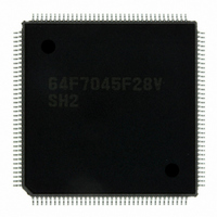
HD64F7045F28V Renesas Electronics America, HD64F7045F28V Datasheet - Page 37

HD64F7045F28V
Manufacturer Part Number
HD64F7045F28V
Description
IC SH2 MCU FLASH 144QFP
Manufacturer
Renesas Electronics America
Series
SuperH® SH7040r
Specifications of HD64F7045F28V
Core Processor
SH-2
Core Size
32-Bit
Speed
28.7MHz
Connectivity
EBI/EMI, SCI
Peripherals
DMA, POR, PWM, WDT
Number Of I /o
98
Program Memory Size
256KB (256K x 8)
Program Memory Type
FLASH
Ram Size
4K x 8
Voltage - Supply (vcc/vdd)
4.5 V ~ 5.5 V
Data Converters
A/D 8x10b
Oscillator Type
Internal
Operating Temperature
-20°C ~ 75°C
Package / Case
144-QFP
Lead Free Status / RoHS Status
Lead free / RoHS Compliant
Eeprom Size
-
Available stocks
Company
Part Number
Manufacturer
Quantity
Price
Company:
Part Number:
HD64F7045F28V
Manufacturer:
Renesas Electronics America
Quantity:
10 000
Part Number:
HD64F7045F28V
Manufacturer:
RENESAS/瑞萨
Quantity:
20 000
- Current page: 37 of 531
- Download datasheet (3Mb)
Section 3 Data Formats
In single data transfers, the A0G and A1G registers can be handled as independent registers. Eight
bits of data can be loaded to or stored from the A0G and A1G registers.
When the A0G or A1G register is the source register, only eight bits are stored from the register.
The top bits are sign extended.
When the A0G or A1G register is the destination register, the bottom eight bits are loaded to the
register. The A0 and A1 registers are not cleared with zeros, so the values are preserved.
Tables 3.1 and 3.2 list the data formats on the register with the DSP instructions. With some
instructions, not all registers can be accessed. For example, the PMULS instruction can specified
the A1 register as the source register, but not the A0 register. For more information, see the
description of the instruction.
Figure 3.5 shows the relationship between the DSP registers and buses during data transfers.
Rev. 5.00 Jun 30, 2004 page 21 of 512
REJ09B0171-0500O
Related parts for HD64F7045F28V
Image
Part Number
Description
Manufacturer
Datasheet
Request
R

Part Number:
Description:
KIT STARTER FOR M16C/29
Manufacturer:
Renesas Electronics America
Datasheet:

Part Number:
Description:
KIT STARTER FOR R8C/2D
Manufacturer:
Renesas Electronics America
Datasheet:

Part Number:
Description:
R0K33062P STARTER KIT
Manufacturer:
Renesas Electronics America
Datasheet:

Part Number:
Description:
KIT STARTER FOR R8C/23 E8A
Manufacturer:
Renesas Electronics America
Datasheet:

Part Number:
Description:
KIT STARTER FOR R8C/25
Manufacturer:
Renesas Electronics America
Datasheet:

Part Number:
Description:
KIT STARTER H8S2456 SHARPE DSPLY
Manufacturer:
Renesas Electronics America
Datasheet:

Part Number:
Description:
KIT STARTER FOR R8C38C
Manufacturer:
Renesas Electronics America
Datasheet:

Part Number:
Description:
KIT STARTER FOR R8C35C
Manufacturer:
Renesas Electronics America
Datasheet:

Part Number:
Description:
KIT STARTER FOR R8CL3AC+LCD APPS
Manufacturer:
Renesas Electronics America
Datasheet:

Part Number:
Description:
KIT STARTER FOR RX610
Manufacturer:
Renesas Electronics America
Datasheet:

Part Number:
Description:
KIT STARTER FOR R32C/118
Manufacturer:
Renesas Electronics America
Datasheet:

Part Number:
Description:
KIT DEV RSK-R8C/26-29
Manufacturer:
Renesas Electronics America
Datasheet:

Part Number:
Description:
KIT STARTER FOR SH7124
Manufacturer:
Renesas Electronics America
Datasheet:

Part Number:
Description:
KIT STARTER FOR H8SX/1622
Manufacturer:
Renesas Electronics America
Datasheet:


