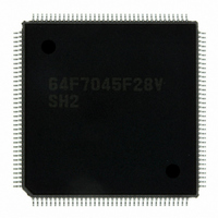
HD64F7045F28V Renesas Electronics America, HD64F7045F28V Datasheet - Page 93

HD64F7045F28V
Manufacturer Part Number
HD64F7045F28V
Description
IC SH2 MCU FLASH 144QFP
Manufacturer
Renesas Electronics America
Series
SuperH® SH7040r
Specifications of HD64F7045F28V
Core Processor
SH-2
Core Size
32-Bit
Speed
28.7MHz
Connectivity
EBI/EMI, SCI
Peripherals
DMA, POR, PWM, WDT
Number Of I /o
98
Program Memory Size
256KB (256K x 8)
Program Memory Type
FLASH
Ram Size
4K x 8
Voltage - Supply (vcc/vdd)
4.5 V ~ 5.5 V
Data Converters
A/D 8x10b
Oscillator Type
Internal
Operating Temperature
-20°C ~ 75°C
Package / Case
144-QFP
Lead Free Status / RoHS Status
Lead free / RoHS Compliant
Eeprom Size
-
Available stocks
Company
Part Number
Manufacturer
Quantity
Price
Company:
Part Number:
HD64F7045F28V
Manufacturer:
Renesas Electronics America
Quantity:
10 000
Part Number:
HD64F7045F28V
Manufacturer:
RENESAS/瑞萨
Quantity:
20 000
- Current page: 93 of 531
- Download datasheet (3Mb)
4.16
The SH-DSP can perform up to two data transfers in parallel between the DSP register and on-
chip memory with the DSP unit. The SH-DSP has the following types of data transfers:
1. X and Y memory data transfers: Data transfer to X and Y memory using the XDB and YDB
2. Single data transfers: Data transfer to on-chip memory using the IDB bus
Note: Data transfer instructions do not update the DSR register’s condition bits.
Table 4.31 shows the various functions.
Table 4.31 Data Transfer Functions
4.16.1
X and Y memory data transfers allow two data transfers to be executed in parallel and allow data
transfers to be executed in parallel with DSP data operations. 32-bit instruction code is required
for executing DSP data operations and transfers in parallel. This is called a parallel data transfer.
When executing an X and Y memory data transfer by itself, 16-bit instruction code is used. This is
called a double data transfer.
Data transfers consist of X memory data transfers and Y memory data transfers. X memory data is
loaded to either the X0 or X1 register; Y memory data is loaded to the Y0 or Y1 register. The X0,
X1, Y0, and Y1 registers become the destination registers. Data can be stored in the X and Y
memory if the A0 or A1 register is the source register. All these data transfers involve word data
Category
X and Y
memory data
transfer
Single data
transfer
buses
•
•
Double data transfer: Data transfer only, where transfer in one direction only is permitted
Parallel data transfers: Data transfer that proceeds in parallel to ALU operation processing
Data Transfers
X and Y Memory Data Transfer
Bus
X bus
Y bus
IDB bus
Length
16 bits
32 bits
16 bits
Parallel Processing
with ALU Operation
None (double)
Available (parallel)
None
Rev. 5.00 Jun 30, 2004 page 77 of 512
Parallel Processing
with Data Transfer
None (X or Y bus)
Available (X and Y
bus)
None (X or Y bus)
Available (X and Y
bus)
None
Section 4 Instruction Features
REJ09B0171-0500O
Instruction
Length
16 bits
16 bits
32 bits
32 bits
16 bits
Related parts for HD64F7045F28V
Image
Part Number
Description
Manufacturer
Datasheet
Request
R

Part Number:
Description:
KIT STARTER FOR M16C/29
Manufacturer:
Renesas Electronics America
Datasheet:

Part Number:
Description:
KIT STARTER FOR R8C/2D
Manufacturer:
Renesas Electronics America
Datasheet:

Part Number:
Description:
R0K33062P STARTER KIT
Manufacturer:
Renesas Electronics America
Datasheet:

Part Number:
Description:
KIT STARTER FOR R8C/23 E8A
Manufacturer:
Renesas Electronics America
Datasheet:

Part Number:
Description:
KIT STARTER FOR R8C/25
Manufacturer:
Renesas Electronics America
Datasheet:

Part Number:
Description:
KIT STARTER H8S2456 SHARPE DSPLY
Manufacturer:
Renesas Electronics America
Datasheet:

Part Number:
Description:
KIT STARTER FOR R8C38C
Manufacturer:
Renesas Electronics America
Datasheet:

Part Number:
Description:
KIT STARTER FOR R8C35C
Manufacturer:
Renesas Electronics America
Datasheet:

Part Number:
Description:
KIT STARTER FOR R8CL3AC+LCD APPS
Manufacturer:
Renesas Electronics America
Datasheet:

Part Number:
Description:
KIT STARTER FOR RX610
Manufacturer:
Renesas Electronics America
Datasheet:

Part Number:
Description:
KIT STARTER FOR R32C/118
Manufacturer:
Renesas Electronics America
Datasheet:

Part Number:
Description:
KIT DEV RSK-R8C/26-29
Manufacturer:
Renesas Electronics America
Datasheet:

Part Number:
Description:
KIT STARTER FOR SH7124
Manufacturer:
Renesas Electronics America
Datasheet:

Part Number:
Description:
KIT STARTER FOR H8SX/1622
Manufacturer:
Renesas Electronics America
Datasheet:


