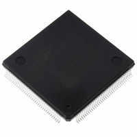
ST10R167-Q3 STMicroelectronics, ST10R167-Q3 Datasheet - Page 40

ST10R167-Q3
Manufacturer Part Number
ST10R167-Q3
Description
IC MCU 16BIT ROMLESS 144-PQFP
Manufacturer
STMicroelectronics
Series
ST10r
Datasheet
1.ST10R167-Q3.pdf
(63 pages)
Specifications of ST10R167-Q3
Core Processor
ST10
Core Size
16-Bit
Speed
25MHz
Connectivity
CAN, EBI/EMI, SSC, UART/USART
Peripherals
POR, PWM, WDT
Number Of I /o
111
Program Memory Type
ROMless
Ram Size
4K x 8
Voltage - Supply (vcc/vdd)
4.5 V ~ 5.5 V
Data Converters
A/D 16x10b
Oscillator Type
Internal
Operating Temperature
-40°C ~ 125°C
Package / Case
144-QFP
Processor Series
ST10R1x
Core
ST10
Data Bus Width
16 bit
Program Memory Size
32 KB
Data Ram Size
4 KB
Interface Type
CAN/SSC/USART
Maximum Clock Frequency
25 MHz
Number Of Programmable I/os
111
Number Of Timers
5
Maximum Operating Temperature
+ 125 C
Mounting Style
SMD/SMT
Minimum Operating Temperature
- 40 C
On-chip Adc
16-ch x 10-bit
Lead Free Status / RoHS Status
Lead free / RoHS Compliant
Eeprom Size
-
Program Memory Size
-
Lead Free Status / Rohs Status
Lead free / RoHS Compliant
Other names
497-2043
Available stocks
Company
Part Number
Manufacturer
Quantity
Price
Company:
Part Number:
ST10R167-Q3
Manufacturer:
ST
Quantity:
556
Company:
Part Number:
ST10R167-Q3
Manufacturer:
STMicroelectronics
Quantity:
10 000
Part Number:
ST10R167-Q3
Manufacturer:
ST
Quantity:
20 000
Company:
Part Number:
ST10R167-Q3/TR
Manufacturer:
STMicroelectronics
Quantity:
10 000
Company:
Part Number:
ST10R167-Q3B0
Manufacturer:
ST
Quantity:
1 343
Part Number:
ST10R167-Q3B0
Manufacturer:
ST
Quantity:
20 000
ST10R167
XX - ELECTRICAL CHARACTERISTICS (continued)
Notes 1. This specification is not valid for outputs which are switched to open drain mode. In this case the respective output will float and the
Figure 8 : Supply/idle current as a function of operating frequency
XX.3.1 - A/D converter characteristics
V
4.0V
Table 16 : A/D converter characteristics
40/63
R
R
DD
TUE
C
V
ASRC
AREF
Symbol
t
t
AIN
AIN
S
C
= 5V
voltage results from the external circuitry.
2. The maximum current may be drawn while the respective signal line remains inactive.
3. The minimum current must be drawn in order to drive the respective signal line active.
4. This specification is only valid during Reset, or during Hold- or Adapt-mode. Port 6 pins are only affected if they are used as CSx
output and the open drain function is not enabled.
5. Partially tested, guaranteed by design characterization.
6. The supply current is a function of the operating frequency. This dependency is illustrated in the figure below. These parameters
are tested at V
7. This parameter is tested including leakage currents. All inputs (including pins configured as inputs) at 0V to 0.1V or at V
to V
8. Overload conditions occur if the standard operating conditions are exceeded, i.e. the voltage on any pin exceeds the specified
range (i.e. V
(see Figure 8).
V
AREF
DD
SR Analog input voltage range
CC Sample time
CC Conversion time
CC Total unadjusted error
SR Internal resistance of reference voltage
SR Internal resistance of analog source
CC ADC input capacitance
, V
10%, V
REF
source
OV
V
= 0V, all outputs (including pins configured as outputs) disconnected.
DDmax
DD
> V
SS
I [mA]
DD
+ 0.1V, V
195
95
and 20MHz CPU clock with all outputs disconnected and all inputs at V
+0.5V or V
10
= 0V
,
T
Parameter
A
SS
OV
= -40 to +125°C
< V
- 0.1V
5
SS
-0.5V). The absolute sum of input overload currents on all port pins may not exceed 50mA
V
AGND
10
V
SS
15
+ 0.2V (see Table 16)
1
2 4
3 4
5
t
t
7
Test Conditions
CC
S
in [ns]
in [ns]
2 7
20
6 7
I
CCmax
I
I
IDmax
CCtyp
I
IDtyp
V
Min.
AGND
25
IL
–
–
–
–
–
–
or V
f
IH
CPU
.
t
t
CC
[MHz]
14 t
S
/ 330 - 0.25
V
/165 - 0.25
CC
4TCL
2 t
Max.
AREF
± 2
33
SC
+ t
S
+
DD
Unit
LSB
– 0.1V
k
k
pF
V


