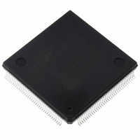
ST10R167-Q3 STMicroelectronics, ST10R167-Q3 Datasheet - Page 41

ST10R167-Q3
Manufacturer Part Number
ST10R167-Q3
Description
IC MCU 16BIT ROMLESS 144-PQFP
Manufacturer
STMicroelectronics
Series
ST10r
Datasheet
1.ST10R167-Q3.pdf
(63 pages)
Specifications of ST10R167-Q3
Core Processor
ST10
Core Size
16-Bit
Speed
25MHz
Connectivity
CAN, EBI/EMI, SSC, UART/USART
Peripherals
POR, PWM, WDT
Number Of I /o
111
Program Memory Type
ROMless
Ram Size
4K x 8
Voltage - Supply (vcc/vdd)
4.5 V ~ 5.5 V
Data Converters
A/D 16x10b
Oscillator Type
Internal
Operating Temperature
-40°C ~ 125°C
Package / Case
144-QFP
Processor Series
ST10R1x
Core
ST10
Data Bus Width
16 bit
Program Memory Size
32 KB
Data Ram Size
4 KB
Interface Type
CAN/SSC/USART
Maximum Clock Frequency
25 MHz
Number Of Programmable I/os
111
Number Of Timers
5
Maximum Operating Temperature
+ 125 C
Mounting Style
SMD/SMT
Minimum Operating Temperature
- 40 C
On-chip Adc
16-ch x 10-bit
Lead Free Status / RoHS Status
Lead free / RoHS Compliant
Eeprom Size
-
Program Memory Size
-
Lead Free Status / Rohs Status
Lead free / RoHS Compliant
Other names
497-2043
Available stocks
Company
Part Number
Manufacturer
Quantity
Price
Company:
Part Number:
ST10R167-Q3
Manufacturer:
ST
Quantity:
556
Company:
Part Number:
ST10R167-Q3
Manufacturer:
STMicroelectronics
Quantity:
10 000
Part Number:
ST10R167-Q3
Manufacturer:
ST
Quantity:
20 000
Company:
Part Number:
ST10R167-Q3/TR
Manufacturer:
STMicroelectronics
Quantity:
10 000
Company:
Part Number:
ST10R167-Q3B0
Manufacturer:
ST
Quantity:
1 343
Part Number:
ST10R167-Q3B0
Manufacturer:
ST
Quantity:
20 000
XX - ELECTRICAL CHARACTERISTICS (continued)
Notes 1. V
Sample time and conversion time of the ST10C167’s ADC are programmable. The table below should be
used to calculate the above timings.
XX.4 - AC characteristics
Test waveforms
Figure 9 : Input output waveforms
Figure 10 : Float waveforms
ADCON.15|14 (ADCTC)
X000
2. During the sample time the input capacitance C
analog source must allow the capacitance to reach its final voltage level within t
analog input voltage have no effect on the conversion result. Values for the sample clock t
from the table above.
3. This parameter includes the sample time t
the conversion result. Values for the conversion clock t
4. This parameter is fixed by ADC control logic.
5. TUE is tested at V
defined voltage range. The specified TUE is guaranteed only if an overload condition (see I
2 not selected analog input pins and the absolute sum of input overload currents on all analog input pins does not exceed 10mA.
During the reset calibration sequence the maximum TUE may be ±4 LSB.
6. During the conversion the ADC’s capacitance must be repeatedly charged or discharged. The internal resistance of the reference
voltage source must allow the capacitance to reach its respective voltage level within t
from the programmed conversion timing.
7. Partially tested, guaranteed by design characterization.
AIN
H
V
0.45V
It begins to float when a 100mV change from the loaded V
or X3FF
2.4V
may exceed V
Load
00
01
10
11
Timing measurements are made at VIH min for a logic ‘1’ and VIL max for a logic ‘0’.
AC inputs during testing are driven at 2.4V for a logic ‘1’ and 0.4V for a logic ‘0’.
For timing purposes a port pin is no longer floating when V
V
H
V
, respectively.
Load
Load
AREF
+0.1V
-0.1V
AGND
= 5.0V, V
or V
Conversion clock t
Reserved, do not use
AREF
AGND
up to the absolute maximum ratings. However, the conversion result in these cases will be
TCL * 24
TCL * 96
TCL * 48
= 0V, V
S
0.2V
0.2V
, the time for determining the digital result and the time to load the result register with
CC
I
DD
DD
= 4.9V. It is guaranteed by design characterization for all other voltages within the
can be charged/discharged by the external source. The internal resistance of the
+0.9
-0.1
CC
CC
Test Points
depend on programming and can be taken from the table above.
Reference
Timing
Points
V
V
OL
OH
ADCON.13|12 (ADSTC)
0.2V
0.2V
OH
DD
DD
/V
00
01
10
+0.9
-0.1
11
S
. After the end of the sample time t
OL
LOAD
level occurs (I
CC
SC
changes of ±100mV.
. The maximum internal resistance results
depend on programming and can be taken
OV
specification) occurs on maximum of
OH
V
/I
Sample clock t
V
OL
OL
OH
= 20mA).
+0.1V
-0.1V
t
t
t
CC
CC
CC
t
CC
S
* 2
* 4
* 8
ST10R167
, changes of the
SC
41/63


