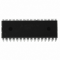
MC908JL16CSPE Freescale Semiconductor, MC908JL16CSPE Datasheet - Page 199

MC908JL16CSPE
Manufacturer Part Number
MC908JL16CSPE
Description
IC MCU 16K FLASH 8MHZ 32-SDIP
Manufacturer
Freescale Semiconductor
Series
HC08r
Datasheet
1.MC908JL16CFJER.pdf
(230 pages)
Specifications of MC908JL16CSPE
Core Processor
HC08
Core Size
8-Bit
Speed
8MHz
Connectivity
I²C, SCI
Peripherals
LED, LVD, POR, PWM
Number Of I /o
26
Program Memory Size
16KB (16K x 8)
Program Memory Type
FLASH
Ram Size
512 x 8
Voltage - Supply (vcc/vdd)
2.7 V ~ 5.5 V
Data Converters
A/D 13x10b
Oscillator Type
Internal
Operating Temperature
-40°C ~ 85°C
Package / Case
32-SDIP (0.400", 10.16mm)
Controller Family/series
HC08
No. Of I/o's
26
Ram Memory Size
512Byte
Cpu Speed
8MHz
No. Of Timers
2
Embedded Interface Type
I2C, SCI
Rohs Compliant
Yes
Processor Series
HC08JL
Core
HC08
Data Bus Width
8 bit
Data Ram Size
512 B
Interface Type
SCI
Maximum Clock Frequency
16 MHz
Number Of Programmable I/os
26
Number Of Timers
4
Operating Supply Voltage
2.7 V to 5.5 V
Maximum Operating Temperature
+ 85 C
Mounting Style
Through Hole
Development Tools By Supplier
FSICEBASE, DEMO908JL16E, M68CBL05CE
Minimum Operating Temperature
- 40 C
On-chip Adc
10 bit, 13 Channel
For Use With
DEMO908JL16E - BOARD DEMO FOR MC908JL16
Lead Free Status / RoHS Status
Lead free / RoHS Compliant
Eeprom Size
-
Lead Free Status / Rohs Status
Details
Available stocks
Company
Part Number
Manufacturer
Quantity
Price
Company:
Part Number:
MC908JL16CSPE
Manufacturer:
SONY
Quantity:
1 560
Part Number:
MC908JL16CSPE
Manufacturer:
FREESCALE
Quantity:
20 000
- Current page: 199 of 230
- Download datasheet (2Mb)
start of boundary address (the page start address: $XX00, $XX40, $XX80, or $00C0) and DATASIZE
must be the same size when accessing the same page.
In some applications, the user may want to repeatedly store and read a set of data from an area of
non-volatile memory. This can be easily implemented when EEPROM memory is used because the byte
erase is allowed in EEPROM. On the other hand in FLASH memory, a minimum erase size is a page (64
bytes), so unused locations in a page will be wasted when it is used for data storage.
The EE_WRITE routine is designed to emulate EEPROM using FLASH. This allows a FLASH page to
implement data storage more efficiently. Each call of the EE_WRITE routine will automatically transfer the
data in the data array (in RAM) to the next available blank locations in a page. Once the page is filled up
with data, the EE_WRITE routine automatically erases the page and programs updated data in the same
page. In a FLASH page, data is programmed to FLASH with in a block that consists of the data array and
one boundary byte. The boundary byte contains the remaining number of bytes which can be
programmed in the page (see
When using this routine to store a 3-byte data array, the FLASH page can be programmed 16 times before
the an erase is required. In effect, the write/erase endurance is increased by 16 times. When a 15-byte
data array is used, the write/erase endurance is increased by 4 times. Due to the FLASH page size
limitation, the data array is limited from 2 bytes to 15 bytes.
The coding example below uses the $EF00–$EE3F page for data storage. The data array size is 15 bytes,
and the bus speed is 4.9152 MHz. The coding assumes the data block is already loaded in RAM, with the
address pointer, FILE_PTR, pointing to the first byte of the data block.
Freescale Semiconductor
ONE PAGE = 64 BYTES
PAGE START
PAGE END
Figure 16-16. EE_WRITE FLASH Memory Usage
Figure
MC68HC908JL16 Data Sheet, Rev. 1.1
16-16).
F
DATA ARRAY
DATA ARRAY
DATA ARRAY
BOUNDARY
BOUNDARY
BOUNDARY
L
A
S
H
$XX00, $XX40, $XX80, OR $XXC0
Monitor Module (MON)
199
Related parts for MC908JL16CSPE
Image
Part Number
Description
Manufacturer
Datasheet
Request
R
Part Number:
Description:
Manufacturer:
Freescale Semiconductor, Inc
Datasheet:
Part Number:
Description:
Manufacturer:
Freescale Semiconductor, Inc
Datasheet:
Part Number:
Description:
Manufacturer:
Freescale Semiconductor, Inc
Datasheet:
Part Number:
Description:
Manufacturer:
Freescale Semiconductor, Inc
Datasheet:
Part Number:
Description:
Manufacturer:
Freescale Semiconductor, Inc
Datasheet:
Part Number:
Description:
Manufacturer:
Freescale Semiconductor, Inc
Datasheet:
Part Number:
Description:
Manufacturer:
Freescale Semiconductor, Inc
Datasheet:
Part Number:
Description:
Manufacturer:
Freescale Semiconductor, Inc
Datasheet:
Part Number:
Description:
Manufacturer:
Freescale Semiconductor, Inc
Datasheet:
Part Number:
Description:
Manufacturer:
Freescale Semiconductor, Inc
Datasheet:
Part Number:
Description:
Manufacturer:
Freescale Semiconductor, Inc
Datasheet:
Part Number:
Description:
Manufacturer:
Freescale Semiconductor, Inc
Datasheet:
Part Number:
Description:
Manufacturer:
Freescale Semiconductor, Inc
Datasheet:
Part Number:
Description:
Manufacturer:
Freescale Semiconductor, Inc
Datasheet:
Part Number:
Description:
Manufacturer:
Freescale Semiconductor, Inc
Datasheet:


