MC908JL16CSPE Freescale Semiconductor, MC908JL16CSPE Datasheet - Page 47
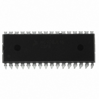
MC908JL16CSPE
Manufacturer Part Number
MC908JL16CSPE
Description
IC MCU 16K FLASH 8MHZ 32-SDIP
Manufacturer
Freescale Semiconductor
Series
HC08r
Datasheet
1.MC908JL16CFJER.pdf
(230 pages)
Specifications of MC908JL16CSPE
Core Processor
HC08
Core Size
8-Bit
Speed
8MHz
Connectivity
I²C, SCI
Peripherals
LED, LVD, POR, PWM
Number Of I /o
26
Program Memory Size
16KB (16K x 8)
Program Memory Type
FLASH
Ram Size
512 x 8
Voltage - Supply (vcc/vdd)
2.7 V ~ 5.5 V
Data Converters
A/D 13x10b
Oscillator Type
Internal
Operating Temperature
-40°C ~ 85°C
Package / Case
32-SDIP (0.400", 10.16mm)
Controller Family/series
HC08
No. Of I/o's
26
Ram Memory Size
512Byte
Cpu Speed
8MHz
No. Of Timers
2
Embedded Interface Type
I2C, SCI
Rohs Compliant
Yes
Processor Series
HC08JL
Core
HC08
Data Bus Width
8 bit
Data Ram Size
512 B
Interface Type
SCI
Maximum Clock Frequency
16 MHz
Number Of Programmable I/os
26
Number Of Timers
4
Operating Supply Voltage
2.7 V to 5.5 V
Maximum Operating Temperature
+ 85 C
Mounting Style
Through Hole
Development Tools By Supplier
FSICEBASE, DEMO908JL16E, M68CBL05CE
Minimum Operating Temperature
- 40 C
On-chip Adc
10 bit, 13 Channel
For Use With
DEMO908JL16E - BOARD DEMO FOR MC908JL16
Lead Free Status / RoHS Status
Lead free / RoHS Compliant
Eeprom Size
-
Lead Free Status / Rohs Status
Details
Available stocks
Company
Part Number
Manufacturer
Quantity
Price
Company:

Part Number:
MC908JL16CSPE
Manufacturer:
SONY
Quantity:
1 560
Part Number:
MC908JL16CSPE
Manufacturer:
FREESCALE
Quantity:
20 000


4.2 SIM Bus Clock Control and Generation
The bus clock generator provides system clock signals for the CPU and peripherals on the MCU. The
system clocks are generated from an incoming clock, OSCOUT, as shown in
4.2.1 Bus Timing
In user mode, the internal bus frequency is the oscillator frequency divided by four.
4.2.2 Clock Start-Up from POR or LVI Reset
When the power-on reset module or the low-voltage inhibit module generates a reset, the clocks to the
CPU and peripherals are inactive and held in an inactive phase until after the 4096 ICLK cycle POR
timeout has completed. The RST pin is driven low by the SIM during this entire period. The IBUS clocks
start upon completion of the timeout.
Freescale Semiconductor
$FE03
$FE04
$FE05
$FE06
Addr.
Interrupt Status Register 1
Interrupt Status Register 2
Interrupt Status Register 3
Register Name
Break Flag Control
Register (BFCR)
XTALCLK / RCCLK
INTERNAL RC
OSCILLATOR
(INT1)
(INT2)
(INT3)
Figure 4-2. SIM I/O Register Summary (Continued)
Reset:
Reset:
Reset:
Reset:
Read:
Read:
Read:
Read:
Write:
Write:
Write:
Write:
BCFE
Bit 7
MC68HC908JL16 Data Sheet, Rev. 1.1
IF14
IF6
Figure 4-3. SIM Clock Signals
R
R
R
0
0
0
0
0
OSC
÷
2
= Unimplemented
IF13
IF5
R
R
R
R
6
0
0
0
0
OSCOUT
ICLK
IF12
IF4
R
R
R
R
5
0
0
0
0
IF11
IF3
R
R
R
R
4
0
0
0
0
÷
SIM COUNTER
2
SIM
SIM Bus Clock Control and Generation
IF10
R
R
R
R
R
3
0
0
0
0
0
GENERATORS
BUS CLOCK
Figure
= Reserved
IF1
R
R
R
R
2
0
0
0
0
0
4-3.
IF8
R
R
R
R
1
0
0
0
0
0
Bit 0
IF15
IF7
R
R
R
R
0
0
0
0
47
Related parts for MC908JL16CSPE
Image
Part Number
Description
Manufacturer
Datasheet
Request
R

Part Number:
Description:
Manufacturer:
Freescale Semiconductor, Inc
Datasheet:
Part Number:
Description:
Manufacturer:
Freescale Semiconductor, Inc
Datasheet:
Part Number:
Description:
Manufacturer:
Freescale Semiconductor, Inc
Datasheet:
Part Number:
Description:
Manufacturer:
Freescale Semiconductor, Inc
Datasheet:
Part Number:
Description:
Manufacturer:
Freescale Semiconductor, Inc
Datasheet:
Part Number:
Description:
Manufacturer:
Freescale Semiconductor, Inc
Datasheet:
Part Number:
Description:
Manufacturer:
Freescale Semiconductor, Inc
Datasheet:
Part Number:
Description:
Manufacturer:
Freescale Semiconductor, Inc
Datasheet:
Part Number:
Description:
Manufacturer:
Freescale Semiconductor, Inc
Datasheet:
Part Number:
Description:
Manufacturer:
Freescale Semiconductor, Inc
Datasheet:
Part Number:
Description:
Manufacturer:
Freescale Semiconductor, Inc
Datasheet:
Part Number:
Description:
Manufacturer:
Freescale Semiconductor, Inc
Datasheet:
Part Number:
Description:
Manufacturer:
Freescale Semiconductor, Inc
Datasheet:
Part Number:
Description:
Manufacturer:
Freescale Semiconductor, Inc
Datasheet:
Part Number:
Description:
Manufacturer:
Freescale Semiconductor, Inc
Datasheet: