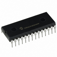
PIC16F57-I/P Microchip Technology, PIC16F57-I/P Datasheet - Page 22

PIC16F57-I/P
Manufacturer Part Number
PIC16F57-I/P
Description
IC MCU FLASH 2KX12 28DIP
Manufacturer
Microchip Technology
Series
PIC® 16Fr
Datasheets
1.PIC16F54-ISS.pdf
(88 pages)
2.PIC16F57-ISS.pdf
(16 pages)
3.PIC16F57-ISO.pdf
(86 pages)
Specifications of PIC16F57-I/P
Program Memory Type
FLASH
Program Memory Size
3KB (2K x 12)
Package / Case
28-DIP (0.600", 15.24mm)
Core Processor
PIC
Core Size
8-Bit
Speed
20MHz
Peripherals
POR, WDT
Number Of I /o
20
Ram Size
72 x 8
Voltage - Supply (vcc/vdd)
2 V ~ 5.5 V
Oscillator Type
External
Operating Temperature
-40°C ~ 85°C
Processor Series
PIC16F
Core
PIC
Data Bus Width
8 bit
Data Ram Size
72 B
Maximum Clock Frequency
20 MHz
Number Of Programmable I/os
20
Number Of Timers
1
Operating Supply Voltage
2 V to 5.5 V
Maximum Operating Temperature
+ 85 C
Mounting Style
Through Hole
3rd Party Development Tools
52715-96, 52716-328, 52717-734
Development Tools By Supplier
DV164120, DV164101, ICE2000
Minimum Operating Temperature
- 40 C
Data Rom Size
2 K
Height
3.3 mm
Length
34.67 mm
Supply Voltage (max)
5.5 V
Supply Voltage (min)
2 V
Width
7.24 mm
Lead Free Status / RoHS Status
Lead free / RoHS Compliant
For Use With
XLT28XP - SOCKET TRANSITION ICE 28DIPAC164001 - MODULE SKT PROMATEII 18/28DIP
Eeprom Size
-
Data Converters
-
Connectivity
-
Lead Free Status / Rohs Status
Lead free / RoHS Compliant
Available stocks
Company
Part Number
Manufacturer
Quantity
Price
Company:
Part Number:
PIC16F57-I/P
Manufacturer:
Microchip Technology
Quantity:
26 657
Part Number:
PIC16F57-I/P
Manufacturer:
MICROCHIP/微芯
Quantity:
20 000
PIC16F5X
3.6
The PIC16F54 device has a 9-bit wide, two-level hard-
ware PUSH/POP stack. The PIC16F57 and PIC16F59
devices have an 11-bit wide, two-level hardware
PUSH/POP stack.
A CALL instruction will PUSH the current value of stack 1
into stack 2 and then PUSH the current program counter
value, incremented by one, into stack level 1. If more than
two sequential CALL’s are executed, only the most recent
two return addresses are stored.
A RETLW instruction will POP the contents of stack level
1 into the program counter and then copy stack level 2
contents into level 1. If more than two sequential
RETLW’s are executed, the stack will be filled with the
address previously stored in level 2.
For the RETLW instruction, the PC is loaded with the
Top-of-Stack (TOS) contents. All of the devices cov-
ered in this data sheet have a two-level stack. The
stack has the same bit width as the device PC, there-
fore, paging is not an issue when returning from a sub-
routine.
3.7
The INDF register is not a physical register. Addressing
INDF actually addresses the register whose address is
contained in the FSR Register (FSR is a pointer). This
is indirect addressing.
DS41213D-page 20
Note:
Stack
Indirect Data Addressing; INDF
and FSR Registers
The W register will be loaded with the
literal value specified in the instruction.
This
implementation of data look-up tables
within the program memory.
is
particularly
useful
for
the
EXAMPLE 3-1:
• Register file 08 contains the value 10h
• Register file 09 contains the value 0Ah
• Load the value 08 into the FSR register
• A read of the INDF register will return the value
• Increment the value of the FSR register by one
• A read of the INDF register now will return the
Reading INDF itself indirectly (FSR = 0) will produce
00h. Writing to the INDF register indirectly results in a
no-operation (although Status bits may be affected).
A simple program to clear RAM locations 10h-1Fh
using indirect addressing is shown in Example 3-2.
EXAMPLE 3-2:
The FSR is either a 5-bit (PIC16F54), 7-bit (PIC16F57)
or 8-bit (PIC16F59) wide register. It is used in conjunc-
tion with the INDF register to indirectly address the data
memory area.
The FSR<4:0> bits are used to select data memory
addresses 00h to 1Fh.
NEXT
CONTINUE
PIC16F54: This does not use banking. FSR<7:5> bits
are unimplemented and read as ‘1’s.
PIC16F57: FSR<7> bit is unimplemented and read as
‘1’. FSR<6:5> are the bank select bits and are used to
select the bank to be addressed (00 = Bank 0,
01 = Bank 1, 10 = Bank 2, 11 = Bank 3).
PIC16F59: FSR<7:5> are the bank select bits and are
used to select the bank to be addressed
(000 = Bank 0, 001 = Bank 1, 010 = Bank 2,
011 = Bank 3, 100 = Bank 4, 101 = Bank 5,
110 = Bank 6, 111 = Bank 7).
of 10h
(FSR = 09h)
value of 0Ah.
Note:
MOVLW H'10'
MOVWF FSR
CLRF
INCF
BTFSC FSR,4
GOTO
:
A CLRF FSR instruction may not result in
an FSR value of 00h if there are
unimplemented bits present in the FSR.
INDF
FSR,F
NEXT
INDIRECT ADDRESSING
HOW TO CLEAR RAM
USING INDIRECT
ADDRESSING
© 2007 Microchip Technology Inc.
;initialize pointer
;to RAM
;clear INDF Register
;inc pointer
;all done?
;NO, clear next
;YES, continue


