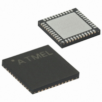
ATMEGA8535-16MU Atmel, ATMEGA8535-16MU Datasheet - Page 210

ATMEGA8535-16MU
Manufacturer Part Number
ATMEGA8535-16MU
Description
IC AVR MCU 8K 16MHZ 5V 44-QFN
Manufacturer
Atmel
Series
AVR® ATmegar
Specifications of ATMEGA8535-16MU
Core Processor
AVR
Core Size
8-Bit
Speed
16MHz
Connectivity
I²C, SPI, UART/USART
Peripherals
Brown-out Detect/Reset, POR, PWM, WDT
Number Of I /o
32
Program Memory Size
8KB (4K x 16)
Program Memory Type
FLASH
Eeprom Size
512 x 8
Ram Size
512 x 8
Voltage - Supply (vcc/vdd)
4.5 V ~ 5.5 V
Data Converters
A/D 8x10b
Oscillator Type
Internal
Operating Temperature
-40°C ~ 85°C
Package / Case
44-VQFN Exposed Pad
Processor Series
ATMEGA8x
Core
AVR8
Data Bus Width
8 bit
Data Ram Size
512 B
Interface Type
2-Wire, SPI, USART
Maximum Clock Frequency
16 MHz
Number Of Programmable I/os
32
Number Of Timers
3
Operating Supply Voltage
4.5 V to 5.5 V
Maximum Operating Temperature
+ 85 C
Mounting Style
SMD/SMT
3rd Party Development Tools
EWAVR, EWAVR-BL
Development Tools By Supplier
ATAVRDRAGON, ATSTK500, ATSTK600, ATAVRISP2, ATAVRONEKIT
Minimum Operating Temperature
- 40 C
On-chip Adc
10 bit, 8 Channel
Package
44MLF EP
Device Core
AVR
Family Name
ATmega
Maximum Speed
16 MHz
For Use With
ATAVRISP2 - PROGRAMMER AVR IN SYSTEMATSTK500 - PROGRAMMER AVR STARTER KIT
Lead Free Status / RoHS Status
Lead free / RoHS Compliant
Available stocks
Company
Part Number
Manufacturer
Quantity
Price
Part Number:
ATMEGA8535-16MU
Manufacturer:
ATMEL/爱特梅尔
Quantity:
20 000
- Current page: 210 of 321
- Download datasheet (3Mb)
210
ATmega8535(L)
The ADC module contains a prescaler, which generates an acceptable ADC clock fre-
quency from any CPU frequency above 100 kHz. The prescaling is set by the ADPS bits
in ADCSRA. The prescaler starts counting from the moment the ADC is switched on by
setting the ADEN bit in ADCSRA. The prescaler keeps running for as long as the ADEN
bit is set, and is continuously reset when ADEN is low.
When initiating a single ended conversion by setting the ADSC bit in ADCSRA, the con-
version starts at the following rising edge of the ADC clock cycle. See “Differential Gain
Channels” on page 212 for details on differential conversion timing.
A normal conversion takes 13 ADC clock cycles. The first conversion after the ADC is
switched on (ADEN in ADCSRA is set) takes 25 ADC clock cycles in order to initialize
the analog circuitry.
The actual sample-and-hold takes place 1.5 ADC clock cycles after the start of a normal
conversion and 13.5 ADC clock cycles after the start of an first conversion. When a con-
version is complete, the result is written to the ADC Data Registers, and ADIF is set. In
Single Conversion mode, ADSC is cleared simultaneously. The software may then set
ADSC again, and a new conversion will be initiated on the first rising ADC clock edge.
When Auto Triggering is used, the prescaler is reset when the trigger event occurs. This
assures a fixed delay from the trigger event to the start of conversion. In this mode, the
sample-and-hold takes place two ADC clock cycles after the rising edge on the trigger
source signal. Three additional CPU clock cycles are used for synchronization logic.
In Free Running mode, a new conversion will be started immediately after the conver-
sion completes, while ADSC remains high. For a summary of conversion times, see
Table 82.
Figure 101. ADC Timing Diagram, First Conversion (Single Conversion Mode)
Cycle Number
ADC Clock
ADEN
ADSC
ADIF
ADCH
ADCL
1
2
MUX and REFS
Update
12
13
14
15
Sample & Hold
16
First Conversion
17
18
19
20
21
22
Conversion
Complete
23
24
25
MSB of Result
Next
Conversion
2502K–AVR–10/06
1
LSB of Result
2
MUX and REFS
Update
3
Related parts for ATMEGA8535-16MU
Image
Part Number
Description
Manufacturer
Datasheet
Request
R

Part Number:
Description:
IC AVR MCU 2.4GHZ XCEIVER 64QFN
Manufacturer:
Atmel
Datasheet:

Part Number:
Description:
Manufacturer:
Atmel
Datasheet:

Part Number:
Description:
MCU ATMEGA644/AT86RF230 40-DIP
Manufacturer:
Atmel
Datasheet:

Part Number:
Description:
BUNDLE ATMEGA644P/AT86RF230 QFN
Manufacturer:
Atmel
Datasheet:

Part Number:
Description:
BUNDLE ATMEGA644P/AT86RF230 TQFP
Manufacturer:
Atmel
Datasheet:

Part Number:
Description:
MCU ATMEGA1281/AT86RF230 64-TQFP
Manufacturer:
Atmel
Datasheet:

Part Number:
Description:
MCU ATMEGA1280/AT86RF230 100TQFP
Manufacturer:
Atmel
Datasheet:

Part Number:
Description:
BUNDLE ATMEGA1280/AT86RF100-TQFP
Manufacturer:
Atmel
Datasheet:

Part Number:
Description:
BUNDLE ATMEGA2560V/AT86RF230-ZU
Manufacturer:
Atmel
Datasheet:

Part Number:
Description:
MCU ATMEGA2561/AT86RF230 64-TQFP
Manufacturer:
Atmel
Datasheet:

Part Number:
Description:
INTERVAL AND WIPE/WASH WIPER CONTROL IC WITH DELAY
Manufacturer:
ATMEL Corporation
Datasheet:

Part Number:
Description:
Low-Voltage Voice-Switched IC for Hands-Free Operation
Manufacturer:
ATMEL Corporation
Datasheet:

Part Number:
Description:
MONOLITHIC INTEGRATED FEATUREPHONE CIRCUIT
Manufacturer:
ATMEL Corporation
Datasheet:

Part Number:
Description:
AM-FM Receiver IC U4255BM-M
Manufacturer:
ATMEL Corporation
Datasheet:


