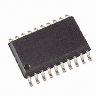
ATTINY2313-20SU Atmel, ATTINY2313-20SU Datasheet - Page 100

ATTINY2313-20SU
Manufacturer Part Number
ATTINY2313-20SU
Description
IC MCU AVR 2K FLASH 20SOIC
Manufacturer
Atmel
Series
AVR® ATtinyr
Specifications of ATTINY2313-20SU
Core Processor
AVR
Core Size
8-Bit
Speed
20MHz
Connectivity
SPI, UART/USART
Peripherals
Brown-out Detect/Reset, POR, PWM, WDT
Number Of I /o
18
Program Memory Size
2KB (1K x 16)
Program Memory Type
FLASH
Eeprom Size
128 x 8
Ram Size
128 x 8
Voltage - Supply (vcc/vdd)
2.7 V ~ 5.5 V
Oscillator Type
Internal
Operating Temperature
-40°C ~ 85°C
Package / Case
20-SOIC (7.5mm Width)
Cpu Family
ATtiny
Device Core
AVR
Device Core Size
8b
Frequency (max)
20MHz
Interface Type
SPI/USART/USI
Total Internal Ram Size
128Byte
# I/os (max)
18
Number Of Timers - General Purpose
2
Operating Supply Voltage (typ)
3.3/5V
Operating Supply Voltage (max)
5.5V
Operating Supply Voltage (min)
2.7V
Instruction Set Architecture
RISC
Operating Temp Range
-40C to 85C
Operating Temperature Classification
Industrial
Mounting
Surface Mount
Pin Count
20
Package Type
SOIC
Package
20SOIC
Family Name
ATtiny
Maximum Speed
20 MHz
Operating Supply Voltage
3.3|5 V
Data Bus Width
8 Bit
Number Of Programmable I/os
18
Number Of Timers
2
Processor Series
ATTINY2x
Core
AVR8
Data Ram Size
128 B
Maximum Clock Frequency
20 MHz
Maximum Operating Temperature
+ 85 C
Mounting Style
SMD/SMT
3rd Party Development Tools
EWAVR, EWAVR-BL
Development Tools By Supplier
ATAVRDRAGON, ATSTK500, ATSTK600, ATAVRISP2, ATAVRONEKIT
Minimum Operating Temperature
- 40 C
Data Rom Size
128 B
Height
2.35 mm
Length
13 mm
Supply Voltage (max)
5.5 V
Supply Voltage (min)
2.7 V
Width
7.6 mm
For Use With
ATSTK600-DIP40 - STK600 SOCKET/ADAPTER 40-PDIP770-1007 - ISP 4PORT ATMEL AVR MCU SPI/JTAG770-1004 - ISP 4PORT FOR ATMEL AVR MCU SPIATAVRDRAGON - KIT DRAGON 32KB FLASH MEM AVRATAVRISP2 - PROGRAMMER AVR IN SYSTEMATJTAGICE2 - AVR ON-CHIP D-BUG SYSTEM
Lead Free Status / RoHS Status
Lead free / RoHS Compliant
Data Converters
-
Lead Free Status / Rohs Status
Compliant
Available stocks
Company
Part Number
Manufacturer
Quantity
Price
Company:
Part Number:
ATTINY2313-20SU
Manufacturer:
ATMEL
Quantity:
441
Company:
Part Number:
ATTINY2313-20SU
Manufacturer:
AT
Quantity:
1 212
Part Number:
ATTINY2313-20SU
Manufacturer:
ATMEL
Quantity:
20 000
Phase and Frequency
Correct PWM Mode
100
ATtiny2313
The phase and frequency correct Pulse Width Modulation, or phase and frequency correct PWM
mode (WGM13:0 = 8 or 9) provides a high resolution phase and frequency correct PWM wave-
form generation option. The phase and frequency correct PWM mode is, like the phase correct
PWM mode, based on a dual-slope operation. The counter counts repeatedly from BOTTOM
(0x0000) to TOP and then from TOP to BOTTOM. In non-inverting Compare Output mode, the
Output Compare (OC1x) is cleared on the compare match between TCNT1 and OCR1x while
upcounting, and set on the compare match while downcounting. In inverting Compare Output
mode, the operation is inverted. The dual-slope operation gives a lower maximum operation fre-
quency compared to the single-slope operation. However, due to the symmetric feature of the
dual-slope PWM modes, these modes are preferred for motor control applications.
The main difference between the phase correct, and the phase and frequency correct PWM
mode is the time the OCR1x Register is updated by the OCR1x Buffer Register, (see
and
The PWM resolution for the phase and frequency correct PWM mode can be defined by either
ICR1 or OCR1A. The minimum resolution allowed is 2-bit (ICR1 or OCR1A set to 0x0003), and
the maximum resolution is 16-bit (ICR1 or OCR1A set to MAX). The PWM resolution in bits can
be calculated using the following equation:
In phase and frequency correct PWM mode the counter is incremented until the counter value
matches either the value in ICR1 (WGM13:0 = 8), or the value in OCR1A (WGM13:0 = 9). The
counter has then reached the TOP and changes the count direction. The TCNT1 value will be
equal to TOP for one timer clock cycle. The timing diagram for the phase correct and frequency
correct PWM mode is shown on
mode when OCR1A or ICR1 is used to define TOP. The TCNT1 value is in the timing diagram
shown as a histogram for illustrating the dual-slope operation. The diagram includes non-
inverted and inverted PWM outputs. The small horizontal line marks on the TCNT1 slopes repre-
sent compare matches between OCR1x and TCNT1. The OC1x interrupt flag will be set when a
compare match occurs.
Figure 48. Phase and Frequency Correct PWM Mode, Timing Diagram
Figure
TCNTn
OCnx
OCnx
Period
48).
1
Figure
R
PFCPWM
2
48. The figure shows phase and frequency correct PWM
=
3
log
---------------------------------- -
(
log
TOP
2 ( )
+
1
4
)
OCnA Interrupt Flag Set
or ICFn Interrupt Flag Set
(Interrupt on TOP)
(COMnx1:0 = 2)
(COMnx1:0 = 3)
OCRnx/TOP Updateand
TOVn Interrupt Flag Set
(Interrupt on Bottom)
2543L–AVR–08/10
Figure 47


