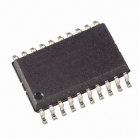
ATTINY2313-20SU Atmel, ATTINY2313-20SU Datasheet - Page 124

ATTINY2313-20SU
Manufacturer Part Number
ATTINY2313-20SU
Description
IC MCU AVR 2K FLASH 20SOIC
Manufacturer
Atmel
Series
AVR® ATtinyr
Specifications of ATTINY2313-20SU
Core Processor
AVR
Core Size
8-Bit
Speed
20MHz
Connectivity
SPI, UART/USART
Peripherals
Brown-out Detect/Reset, POR, PWM, WDT
Number Of I /o
18
Program Memory Size
2KB (1K x 16)
Program Memory Type
FLASH
Eeprom Size
128 x 8
Ram Size
128 x 8
Voltage - Supply (vcc/vdd)
2.7 V ~ 5.5 V
Oscillator Type
Internal
Operating Temperature
-40°C ~ 85°C
Package / Case
20-SOIC (7.5mm Width)
Cpu Family
ATtiny
Device Core
AVR
Device Core Size
8b
Frequency (max)
20MHz
Interface Type
SPI/USART/USI
Total Internal Ram Size
128Byte
# I/os (max)
18
Number Of Timers - General Purpose
2
Operating Supply Voltage (typ)
3.3/5V
Operating Supply Voltage (max)
5.5V
Operating Supply Voltage (min)
2.7V
Instruction Set Architecture
RISC
Operating Temp Range
-40C to 85C
Operating Temperature Classification
Industrial
Mounting
Surface Mount
Pin Count
20
Package Type
SOIC
Package
20SOIC
Family Name
ATtiny
Maximum Speed
20 MHz
Operating Supply Voltage
3.3|5 V
Data Bus Width
8 Bit
Number Of Programmable I/os
18
Number Of Timers
2
Processor Series
ATTINY2x
Core
AVR8
Data Ram Size
128 B
Maximum Clock Frequency
20 MHz
Maximum Operating Temperature
+ 85 C
Mounting Style
SMD/SMT
3rd Party Development Tools
EWAVR, EWAVR-BL
Development Tools By Supplier
ATAVRDRAGON, ATSTK500, ATSTK600, ATAVRISP2, ATAVRONEKIT
Minimum Operating Temperature
- 40 C
Data Rom Size
128 B
Height
2.35 mm
Length
13 mm
Supply Voltage (max)
5.5 V
Supply Voltage (min)
2.7 V
Width
7.6 mm
For Use With
ATSTK600-DIP40 - STK600 SOCKET/ADAPTER 40-PDIP770-1007 - ISP 4PORT ATMEL AVR MCU SPI/JTAG770-1004 - ISP 4PORT FOR ATMEL AVR MCU SPIATAVRDRAGON - KIT DRAGON 32KB FLASH MEM AVRATAVRISP2 - PROGRAMMER AVR IN SYSTEMATJTAGICE2 - AVR ON-CHIP D-BUG SYSTEM
Lead Free Status / RoHS Status
Lead free / RoHS Compliant
Data Converters
-
Lead Free Status / Rohs Status
Compliant
Available stocks
Company
Part Number
Manufacturer
Quantity
Price
Company:
Part Number:
ATTINY2313-20SU
Manufacturer:
ATMEL
Quantity:
441
Company:
Part Number:
ATTINY2313-20SU
Manufacturer:
AT
Quantity:
1 212
Part Number:
ATTINY2313-20SU
Manufacturer:
ATMEL
Quantity:
20 000
Parity Checker
Disabling the Receiver In contrast to the Transmitter, disabling of the Receiver will be immediate. Data from ongoing
Flushing the Receive
Buffer
Asynchronous
Data Reception
124
ATtiny2313
The Parity Checker is active when the high USART Parity mode (UPM1) bit is set. Type of Parity
Check to be performed (odd or even) is selected by the UPM0 bit. When enabled, the Parity
Checker calculates the parity of the data bits in incoming frames and compares the result with
the parity bit from the serial frame. The result of the check is stored in the receive buffer together
with the received data and stop bits. The Parity Error (UPE) flag can then be read by software to
check if the frame had a Parity Error.
The UPE bit is set if the next character that can be read from the receive buffer had a Parity
Error when received and the Parity Checking was enabled at that point (UPM1 = 1). This bit is
valid until the receive buffer (UDR) is read.
receptions will therefore be lost. When disabled (i.e., the RXEN is set to zero) the Receiver will
no longer override the normal function of the RxD port pin. The Receiver buffer FIFO will be
flushed when the Receiver is disabled. Remaining data in the buffer will be lost
The receiver buffer FIFO will be flushed when the Receiver is disabled, i.e., the buffer will be
emptied of its contents. Unread data will be lost. If the buffer has to be flushed during normal
operation, due to for instance an error condition, read the UDR I/O location until the RXC flag is
cleared. The following code example shows how to flush the receive buffer.
Note:
The USART includes a clock recovery and a data recovery unit for handling asynchronous data
reception. The clock recovery logic is used for synchronizing the internally generated baud rate
clock to the incoming asynchronous serial frames at the RxD pin. The data recovery logic sam-
ples and low pass filters each incoming bit, thereby improving the noise immunity of the
Receiver. The asynchronous reception operational range depends on the accuracy of the inter-
nal baud rate clock, the rate of the incoming frames, and the frame size in number of bits.
Assembly Code Example
C Code Example
USART_Flush:
void USART_Flush( void )
{
}
sbis UCSRA, RXC
ret
in
rjmp USART_Flush
unsigned char dummy;
while ( UCSRA & (1<<RXC) ) dummy = UDR;
1. The example code assumes that the part specific header file is included.
For I/O Registers located in extended I/O map, “IN”, “OUT”, “SBIS”, “SBIC”, “CBI”, and “SBI”
instructions must be replaced with instructions that allow access to extended I/O. Typically
“LDS” and “STS” combined with “SBRS”, “SBRC”, “SBR”, and “CBR”.
r16, UDR
(1)
(1)
2543L–AVR–08/10


