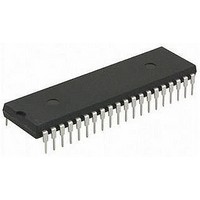
PIC16LF707-I/P Microchip Technology, PIC16LF707-I/P Datasheet - Page 156

PIC16LF707-I/P
Manufacturer Part Number
PIC16LF707-I/P
Description
MCU 8BIT 14KB FLASH 5.5V 40PDIP
Manufacturer
Microchip Technology
Series
PIC® XLP™ 16Fr
Specifications of PIC16LF707-I/P
Core Size
8-Bit
Program Memory Size
14KB (8K x 14)
Peripherals
Brown-out Detect/Reset, POR, PWM, WDT
Core Processor
PIC
Speed
20MHz
Connectivity
I²C, SPI, UART/USART
Number Of I /o
36
Program Memory Type
FLASH
Ram Size
363 x 8
Voltage - Supply (vcc/vdd)
1.8 V ~ 3.6 V
Data Converters
A/D 14x8b
Oscillator Type
Internal
Operating Temperature
-40°C ~ 85°C
Package / Case
40-DIP (0.600", 15.24mm)
Controller Family/series
PIC16LF
No. Of I/o's
36
Ram Memory Size
363Byte
Cpu Speed
20MHz
No. Of Timers
6
Processor Series
PIC16LF
Core
PIC
Data Bus Width
8 bit
Data Ram Size
368 B
Interface Type
I2C, SPI, AUSART
Maximum Clock Frequency
20 MHz
Number Of Programmable I/os
36
Number Of Timers
4
Operating Supply Voltage
1.8 V to 3.6 V
Maximum Operating Temperature
+ 85 C
Mounting Style
Through Hole
3rd Party Development Tools
52715-96, 52716-328, 52717-734
Development Tools By Supplier
PG164130, DV164035, DV244005, DV164005, PG164120, ICE2000
Minimum Operating Temperature
- 40 C
On-chip Adc
8 bit, 14 Channel
On-chip Dac
5 bit
Lead Free Status / RoHS Status
Lead free / RoHS Compliant
Eeprom Size
-
Lead Free Status / Rohs Status
Details
Available stocks
Company
Part Number
Manufacturer
Quantity
Price
Company:
Part Number:
PIC16LF707-I/PT
Manufacturer:
Microchip Technology
Quantity:
10 000
- Current page: 156 of 284
- Download datasheet (3Mb)
PIC16F707/PIC16LF707
18.4
The AUSART will remain active during Sleep only in the
Synchronous Slave mode. All other modes require the
system clock and therefore cannot generate the
necessary signals to run the transmit or receive shift
registers during Sleep.
Synchronous Slave mode uses an externally generated
clock to run the transmit and receive shift registers.
18.4.1
To receive during Sleep, all the following conditions
must be met before entering Sleep mode:
• RCSTA and TXSTA control registers must be
• If interrupts are desired, set the RCIE bit of the
• The RCIF interrupt flag must be cleared by read-
Upon entering Sleep mode, the device will be ready to
accept data and clocks on the RX/DT and TX/CK pins,
respectively. When the data word has been completely
clocked in by the external device, the RCIF interrupt
flag bit of the PIR1 register will be set. Thereby, waking
the processor from Sleep.
Upon waking from Sleep, the instruction following the
SLEEP instruction will be executed. If the Global
Interrupt Enable (GIE) bit of the INTCON register is
also set, then the Interrupt Service Routine at address
0004h will be called.
DS41418A-page 156
configured for synchronous slave reception (refer
to Section 18.3.2.4 “Synchronous Slave
Reception Set-up:”).
PIE1 register and the PEIE bit of the INTCON
register.
ing RCREG to unload any pending characters in
the receive buffer.
AUSART Operation During Sleep
SYNCHRONOUS RECEIVE DURING
SLEEP
Preliminary
18.4.2
To transmit during Sleep, all the following conditions
must be met before entering Sleep mode:
• RCSTA and TXSTA control registers must be
• The TXIF interrupt flag must be cleared by writing
• If interrupts are desired, set the TXIE bit of the
Upon entering Sleep mode, the device will be ready to
accept clocks on TX/CK pin and transmit data on the
RX/DT pin. When the data word in the TSR has been
completely clocked out by the external device, the
pending byte in the TXREG will transfer to the TSR and
the TXIF flag will be set. Thereby, waking the processor
from Sleep. At this point, the TXREG is available to
accept another character for transmission, which will
clear the TXIF flag.
Upon waking from Sleep, the instruction following the
SLEEP instruction will be executed. If the Global
Interrupt Enable (GIE) bit is also set then the Interrupt
Service Routine at address 0004h will be called.
configured for synchronous slave transmission
(refer to Section 18.3.2.2 “Synchronous Slave
Transmission Set-up:”).
the output data to the TXREG, thereby filling the
TSR and transmit buffer.
PIE1 register and the PEIE bit of the INTCON
register.
SYNCHRONOUS TRANSMIT
DURING SLEEP
2010 Microchip Technology Inc.
Related parts for PIC16LF707-I/P
Image
Part Number
Description
Manufacturer
Datasheet
Request
R

Part Number:
Description:
Manufacturer:
Microchip Technology Inc.
Datasheet:

Part Number:
Description:
Manufacturer:
Microchip Technology Inc.
Datasheet:

Part Number:
Description:
Manufacturer:
Microchip Technology Inc.
Datasheet:

Part Number:
Description:
Manufacturer:
Microchip Technology Inc.
Datasheet:

Part Number:
Description:
Manufacturer:
Microchip Technology Inc.
Datasheet:

Part Number:
Description:
Manufacturer:
Microchip Technology Inc.
Datasheet:

Part Number:
Description:
Manufacturer:
Microchip Technology Inc.
Datasheet:

Part Number:
Description:
Manufacturer:
Microchip Technology Inc.
Datasheet:


