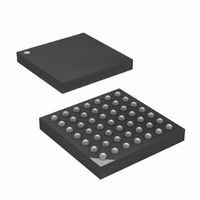
ATXMEGA32A4-CUR Atmel, ATXMEGA32A4-CUR Datasheet - Page 241

ATXMEGA32A4-CUR
Manufacturer Part Number
ATXMEGA32A4-CUR
Description
MCU AVR 32+4 FLASH 49VFBGA
Manufacturer
Atmel
Series
AVR® XMEGAr
Specifications of ATXMEGA32A4-CUR
Core Processor
AVR
Core Size
8/16-Bit
Speed
32MHz
Connectivity
I²C, IrDA, SPI, UART/USART
Peripherals
Brown-out Detect/Reset, DMA, POR, PWM, WDT
Number Of I /o
34
Program Memory Size
32KB (16K x 16)
Program Memory Type
FLASH
Eeprom Size
2K x 8
Ram Size
4K x 8
Voltage - Supply (vcc/vdd)
1.6 V ~ 3.6 V
Data Converters
A/D 12x12b, D/A 2x12b
Oscillator Type
Internal
Operating Temperature
-40°C ~ 85°C
Package / Case
49-VFBGA
For Use With
ATAVRONEKIT - KIT AVR/AVR32 DEBUGGER/PROGRMMRATSTK600 - DEV KIT FOR AVR/AVR32770-1007 - ISP 4PORT ATMEL AVR MCU SPI/JTAG770-1004 - ISP 4PORT FOR ATMEL AVR MCU SPI
Lead Free Status / RoHS Status
Lead free / RoHS Compliant
Available stocks
Company
Part Number
Manufacturer
Quantity
Price
- Current page: 241 of 445
- Download datasheet (6Mb)
21.4.1
21.4.2
21.5
21.6
21.6.1
8077H–AVR–12/09
USART Initialization
Data Transmission - The USART Transmitter
Parity Bit Calculation
SPI Frame Formats
Sending Frames
Table 1.
Even or odd parity can be selected for error checking. If even parity is selected, the parity bit is
set to one if the number of data bits that is one is odd (making the total number of ones even). If
odd parity is selected, the parity bit is set to one if the number of data bits that is one is even
(making the total number of ones odd).
The serial frame in SPI mode is defined to be one character of 8 data bits. The USART in Master
SPI mode has two valid frame formats:
When a complete frame of 8 bits is transmitted, a new frame can directly follow it, or the commu-
nication line returns to idle (high) state.
USART initialization should use the following sequence:
For interrupt driven USART operation, global interrupts should be disabled during the
initialization.
Before doing a re-initialization with changed baud rate or frame format, be sure that there are no
ongoing transmissions during the period the registers are changed. The transit and receive com-
plete interrupt flags can be used to check that the Transmitter has completed all transfers, and
that there are no unread data in the receive buffer.
When the Transmitter has been enabled, the normal port operation of the TxD pin is overridden
by the USART and given the function as the Transmitter's serial output. The direction of the pin
must be set as output using the Direction register in the corresponding port. For details on port
pin control refer to
A data transmission is initiated by loading the transmit buffer (DATA) with the data to be sent.
The data in the transmit buffer is moved to the Shift Register when the Shift Register is empty
and ready to send a new frame. The Shift Register is loaded if it is in idle state (no ongoing
St
(n)
P
Sp
IDLE
• 8-bit data with MSB first
• 8-bit data with LSB first
1. Set the TxD pin value high, and optionally the XCK pin low.
2. Set the TxD and optionally the XCK pin as output.
3. Set the baud rate and frame format.
4. Set mode of operation (enables the XCK pin output in synchronous mode).
5. Enable the Transmitter or the Receiver depending on the usage.
Start bit, always low.
Data bits (0 to 8).
Parity bit. Can be odd or even.
Stop bit, always high.
No transfers on the communication line (RxD or TxD). The IDLE state is always high.
”I/O Ports” on page
129.
XMEGA A
241
Related parts for ATXMEGA32A4-CUR
Image
Part Number
Description
Manufacturer
Datasheet
Request
R

Part Number:
Description:
DEV KIT FOR AVR/AVR32
Manufacturer:
Atmel
Datasheet:

Part Number:
Description:
INTERVAL AND WIPE/WASH WIPER CONTROL IC WITH DELAY
Manufacturer:
ATMEL Corporation
Datasheet:

Part Number:
Description:
Low-Voltage Voice-Switched IC for Hands-Free Operation
Manufacturer:
ATMEL Corporation
Datasheet:

Part Number:
Description:
MONOLITHIC INTEGRATED FEATUREPHONE CIRCUIT
Manufacturer:
ATMEL Corporation
Datasheet:

Part Number:
Description:
AM-FM Receiver IC U4255BM-M
Manufacturer:
ATMEL Corporation
Datasheet:

Part Number:
Description:
Monolithic Integrated Feature Phone Circuit
Manufacturer:
ATMEL Corporation
Datasheet:

Part Number:
Description:
Multistandard Video-IF and Quasi Parallel Sound Processing
Manufacturer:
ATMEL Corporation
Datasheet:

Part Number:
Description:
High-performance EE PLD
Manufacturer:
ATMEL Corporation
Datasheet:

Part Number:
Description:
8-bit Flash Microcontroller
Manufacturer:
ATMEL Corporation
Datasheet:

Part Number:
Description:
2-Wire Serial EEPROM
Manufacturer:
ATMEL Corporation
Datasheet:


