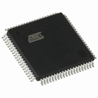
AT89C5132-RORUL Atmel, AT89C5132-RORUL Datasheet - Page 12

AT89C5132-RORUL
Manufacturer Part Number
AT89C5132-RORUL
Description
MCU 8051 FLASH USB 80TQFP
Manufacturer
Atmel
Series
AT89C513xr
Specifications of AT89C5132-RORUL
Core Processor
C52X2
Core Size
8-Bit
Speed
20MHz
Connectivity
IDE/ATAPI, I²C, MMC, PCM, SPI, UART/USART, USB
Peripherals
I²S, POR, WDT
Number Of I /o
44
Program Memory Size
64KB (64K x 8)
Program Memory Type
FLASH
Eeprom Size
4K x 8
Ram Size
2.25K x 8
Voltage - Supply (vcc/vdd)
2.7 V ~ 3.3 V
Data Converters
A/D 2x10b
Oscillator Type
Internal
Operating Temperature
-40°C ~ 85°C
Package / Case
80-TQFP, 80-VQFP
Lead Free Status / RoHS Status
Lead free / RoHS Compliant
Available stocks
Company
Part Number
Manufacturer
Quantity
Price
- Current page: 12 of 182
- Download datasheet (2Mb)
6. Clock Controller
6.1
6.2
12
Oscillator
X2 Feature
AT89C5132
The AT89C5132 clock controller is based on an on-chip oscillator feeding an on-chip Phase
Lock Loop (PLL). All internal clocks to the peripherals and CPU core are generated by this
controller.
The AT89C5132 X1 and X2 pins are the input and the output of a single-stage on-chip inverter
(see Figure 6-1) that can be configured with off-chip components such as a Pierce oscillator
(see Figure 6-2). Value of capacitors and crystal characteristics are detailed in the Section “DC
Characteristics”.
The oscillator outputs three different clocks: a clock for the PLL, a clock for the CPU core, and a
clock for the peripherals as shown in Figure 6-1. These clocks are either enabled or disabled,
depending on the power reduction mode as detailed in the
page
Port sampling clocks.
Figure 6-1.
Figure 6-2.
Unlike standard C51 products that require 12 oscillator clock periods per machine cycle, the
AT89C5132 needs only 6 oscillator clock periods per machine cycle. This feature called the “X2
feature” can be enabled using the X2 bit
to operate in 6 or 12 oscillator clock periods per machine cycle. As shown in Figure 6-1, both
CPU and peripheral clocks are affected by this feature. Figure 6-3 shows the X2 mode switching
waveforms. After reset, the standard mode is activated. In standard mode, the CPU and periph-
44. The peripheral clock is used to generate the Timer 0, Timer 1, MMC, ADC, SPI, and
X1
X2
Oscillator Block Diagram and Symbol
Crystal Connection
Peripheral Clock Symbol
CLOCK
PCON.1
PER
PD
V
SS
(1)
CPU Core Clock Symbol
in CKCON (see Table 1) and allows the AT89C5132
C1
C2
÷
2
CLOCK
CPU
CKCON.0
Q
X2
0
1
X1
X2
section“Power Management” on
PCON.0
IDL
Oscillator Clock Symbol
CLOCK
OSC
Peripheral
Clock
CPU Core
Clock
Oscillator
Clock
4173E–USB–09/07
Related parts for AT89C5132-RORUL
Image
Part Number
Description
Manufacturer
Datasheet
Request
R

Part Number:
Description:
Manufacturer:
Atmel Corporation
Datasheet:

Part Number:
Description:
IC 8051 MCU FLASH 64K USB 80TQFP
Manufacturer:
Atmel
Datasheet:

Part Number:
Description:
DEV KIT FOR AVR/AVR32
Manufacturer:
Atmel
Datasheet:

Part Number:
Description:
INTERVAL AND WIPE/WASH WIPER CONTROL IC WITH DELAY
Manufacturer:
ATMEL Corporation
Datasheet:

Part Number:
Description:
Low-Voltage Voice-Switched IC for Hands-Free Operation
Manufacturer:
ATMEL Corporation
Datasheet:

Part Number:
Description:
MONOLITHIC INTEGRATED FEATUREPHONE CIRCUIT
Manufacturer:
ATMEL Corporation
Datasheet:

Part Number:
Description:
AM-FM Receiver IC U4255BM-M
Manufacturer:
ATMEL Corporation
Datasheet:

Part Number:
Description:
Monolithic Integrated Feature Phone Circuit
Manufacturer:
ATMEL Corporation
Datasheet:

Part Number:
Description:
Multistandard Video-IF and Quasi Parallel Sound Processing
Manufacturer:
ATMEL Corporation
Datasheet:

Part Number:
Description:
High-performance EE PLD
Manufacturer:
ATMEL Corporation
Datasheet:

Part Number:
Description:
8-bit Flash Microcontroller
Manufacturer:
ATMEL Corporation
Datasheet:


