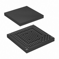
AT91SAM9G20B-CFU Atmel, AT91SAM9G20B-CFU Datasheet - Page 14

AT91SAM9G20B-CFU
Manufacturer Part Number
AT91SAM9G20B-CFU
Description
IC MCU ARM9 247-LFBGA
Manufacturer
Atmel
Series
AT91SAMr
Datasheet
1.AT91SAM9G20B-CU.pdf
(42 pages)
Specifications of AT91SAM9G20B-CFU
Core Processor
ARM9
Core Size
16/32-Bit
Speed
400MHz
Connectivity
EBI/EMI, Ethernet, I²C, IrDA, ISI, MMC, SPI, SSC, UART/USART, USB
Peripherals
DMA, POR, PWM, WDT
Number Of I /o
96
Program Memory Size
64KB (64K x 8)
Program Memory Type
ROM
Ram Size
96K x 8
Voltage - Supply (vcc/vdd)
0.9 V ~ 1.1 V
Data Converters
A/D 4x10b
Oscillator Type
Internal
Operating Temperature
-40°C ~ 85°C
Package / Case
247-TFBGA
Processor Series
AT91SAMx
Core
ARM926EJ-S
Data Bus Width
32 bit
Data Ram Size
16 KB
Interface Type
SPI, TWI, UART
Maximum Clock Frequency
400 MHz
Number Of Programmable I/os
96
Operating Supply Voltage
3.3 V
Maximum Operating Temperature
+ 85 C
Mounting Style
SMD/SMT
3rd Party Development Tools
JTRACE-ARM-2M, MDK-ARM, RL-ARM, ULINK2
Development Tools By Supplier
AT91SAM-ICE, AT91-ISP, AT91SAM9G20-EK
Minimum Operating Temperature
- 40 C
Lead Free Status / RoHS Status
Lead free / RoHS Compliant
Eeprom Size
-
Lead Free Status / Rohs Status
Details
Available stocks
Company
Part Number
Manufacturer
Quantity
Price
6. I/O Line Considerations
6.1
6.2
6.3
6.4
6.5
6.6
14
JTAG Port Pins
Test Pin
Reset Pins
PIO Controllers
I/O Line Drive Levels
Shutdown Logic Pins
AT91SAM9G20 Summary
TMS, TDI and TCK are schmitt trigger inputs and have no pull-up resistors.
TDO and RTCK are outputs, driven at up to VDDIOP, and have no pull-up resistor.
The JTAGSEL pin is used to select the JTAG boundary scan when asserted at a high level. It
integrates a permanent pull-down resistor of about 15 kΩ to GND, so that it can be left uncon-
nected for normal operations.
The NTRST signal is described in the Reset Pins paragraph.
All the JTAG signals are supplied with VDDIOP.
The TST pin is used for manufacturing test purposes when asserted high. It integrates a perma-
nent pull-down resistor of about 15 kΩ to GNDBU, so that it can be left unconnected for normal
operations. Driving this line at a high level leads to unpredictable results.
This pin is supplied with VDDBU.
NRST is an open-drain output integrating a non-programmable pull-up resistor. It can be driven
with voltage at up to VDDIOP.
NTRST is an input which allows reset of the JTAG Test Access port. It has no action on the
processor.
As the product integrates power-on reset cells, which manages the processor and the JTAG
reset, the NRST and NTRST pins can be left unconnected.
The NRST and NTRST pins both integrate a permanent pull-up resistor of 100 kΩ minimum to
VDDIOP.
The NRST signal is inserted in the Boundary Scan.
All the I/O lines are Schmitt trigger inputs and all the lines managed by the PIO Controllers inte-
grate a programmable pull-up resistor of 75 kΩ typical with the exception of P4 - P31. For details,
refer to the section “AT91SAM9G20 Electrical Characteristics”. Programming of this pull-up
resistor is performed independently for each I/O line through the PIO Controllers.
The PIO lines drive current capability is described in the DC Characteristics section of the prod-
uct datasheet.
The SHDN pin is a tri-state output only pin, which is driven by the Shutdown Controller. There is
no internal pull-up. An external pull-up to VDDBU is needed and its value must be higher than 1
MΩ. The resisitor value is calculated according to the regulator enable implementation and the
SHDN level.
The pin WKUP is an input-only. It can accept voltages only between 0V and VDDBU.
6384DS–ATARM–13-Jan-10


