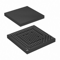
AT91SAM9G20B-CFU Atmel, AT91SAM9G20B-CFU Datasheet - Page 2

AT91SAM9G20B-CFU
Manufacturer Part Number
AT91SAM9G20B-CFU
Description
IC MCU ARM9 247-LFBGA
Manufacturer
Atmel
Series
AT91SAMr
Datasheet
1.AT91SAM9G20B-CU.pdf
(42 pages)
Specifications of AT91SAM9G20B-CFU
Core Processor
ARM9
Core Size
16/32-Bit
Speed
400MHz
Connectivity
EBI/EMI, Ethernet, I²C, IrDA, ISI, MMC, SPI, SSC, UART/USART, USB
Peripherals
DMA, POR, PWM, WDT
Number Of I /o
96
Program Memory Size
64KB (64K x 8)
Program Memory Type
ROM
Ram Size
96K x 8
Voltage - Supply (vcc/vdd)
0.9 V ~ 1.1 V
Data Converters
A/D 4x10b
Oscillator Type
Internal
Operating Temperature
-40°C ~ 85°C
Package / Case
247-TFBGA
Processor Series
AT91SAMx
Core
ARM926EJ-S
Data Bus Width
32 bit
Data Ram Size
16 KB
Interface Type
SPI, TWI, UART
Maximum Clock Frequency
400 MHz
Number Of Programmable I/os
96
Operating Supply Voltage
3.3 V
Maximum Operating Temperature
+ 85 C
Mounting Style
SMD/SMT
3rd Party Development Tools
JTRACE-ARM-2M, MDK-ARM, RL-ARM, ULINK2
Development Tools By Supplier
AT91SAM-ICE, AT91-ISP, AT91SAM9G20-EK
Minimum Operating Temperature
- 40 C
Lead Free Status / RoHS Status
Lead free / RoHS Compliant
Eeprom Size
-
Lead Free Status / Rohs Status
Details
Available stocks
Company
Part Number
Manufacturer
Quantity
Price
•
•
•
•
•
•
•
•
•
•
•
•
•
•
•
•
2
Periodic Interval Timer (PIT)
Watchdog Timer (WDT)
Real-time Timer (RTT)
One 4-channel 10-bit Analog-to-Digital Converter
Three 32-bit Parallel Input/Output Controllers (PIOA, PIOB, PIOC)
Peripheral DMA Controller Channels (PDC)
One Two-slot MultiMedia Card Interface (MCI)
One Synchronous Serial Controller (SSC)
Four Universal Synchronous/Asynchronous Receiver Transmitters (USART)
Two 2-wire UARTs
Two Master/Slave Serial Peripheral Interfaces (SPI)
Two Three-channel 16-bit Timer/Counters (TC)
One Two-wire Interface (TWI)
IEEE
Required Power Supplies
Available in a 217-ball LFBGA and 247-ball TFBGA RoHS-compliant Package
– 20-bit Interval Timer plus 12-bit Interval Counter
– Key-protected, Programmable Only Once, Windowed 16-bit Counter Running at Slow Clock
– 32-bit Free-running Backup Counter Running at Slow Clock with 16-bit Prescaler
– 96 Programmable I/O Lines Multiplexed with up to Two Peripheral I/Os
– Input Change Interrupt Capability on Each I/O Line
– Individually Programmable Open-drain, Pull-up Resistor and Synchronous Output
– All I/O Lines are Schmitt Trigger Inputs
– SDCard/SDIO and MultiMediaCard
– Automatic Protocol Control and Fast Automatic Data Transfers with PDC
– Independent Clock and Frame Sync Signals for Each Receiver and Transmitter
– I²S Analog Interface Support, Time Division Multiplex Support
– High-speed Continuous Data Stream Capabilities with 32-bit Data Transfer
– Individual Baud Rate Generator, IrDA
– Support for ISO7816 T0/T1 Smart Card, Hardware Handshaking, RS485 Support
– Full Modem Signal Control on USART0
– 8- to 16-bit Programmable Data Length, Four External Peripheral Chip Selects
– Synchronous Communications
– Three External Clock Inputs, Two Multi-purpose I/O Pins per Channel
– Double PWM Generation, Capture/Waveform Mode, Up/Down Capability
– High-Drive Capability on Outputs TIOA0, TIOA1, TIOA2
– Compatible with Standard Two-wire Serial Memories
– One, Two or Three Bytes for Slave Address
– Sequential Read/Write Operations
– Master, Multi-master and Slave Mode Operation
– Bit Rate: Up to 400 Kbits
– General Call Supported in Slave Mode
– Connection to Peripheral DMA Controller (PDC) Channel Capabilities Optimizes Data Transfers in Master Mode
– 0.9V to 1.1V for VDDBU, VDDCORE, VDDPLL
– 1.65 to 3.6V for VDDOSC
– 1.65V to 3.6V for VDDIOP (Peripheral I/Os)
– 3.0V to 3.6V for VDDUSB
– 3.0V to 3.6V VDDANA (Analog-to-digital Converter)
– Programmable 1.65V to 1.95V or 3.0V to 3.6V for VDDIOM (Memory I/Os)
®
1149.1 JTAG Boundary Scan on All Digital Pins
AT91SAM9G20 Summary
™
Compliant
®
Infrared Modulation/Demodulation, Manchester Encoding/Decoding
6384DS–ATARM–13-Jan-10


