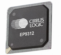
EP9312-CBZ Cirrus Logic Inc, EP9312-CBZ Datasheet - Page 287

EP9312-CBZ
Manufacturer Part Number
EP9312-CBZ
Description
IC ARM9 SOC UNIVERSAL 352PBGA
Manufacturer
Cirrus Logic Inc
Series
EP9r
Specifications of EP9312-CBZ
Core Size
16/32-Bit
Core Processor
ARM9
Speed
200MHz
Connectivity
EBI/EMI, EIDE, Ethernet, I²C, IrDA, Keypad/Touchscreen, SPI, UART/USART, USB
Peripherals
AC'97, DMA, I²:S, LCD, LED, MaverickKey, POR, PWM, WDT
Number Of I /o
16
Program Memory Type
ROMless
Ram Size
32K x 8
Voltage - Supply (vcc/vdd)
1.65 V ~ 3.6 V
Data Converters
A/D 8x12b
Oscillator Type
External
Operating Temperature
0°C ~ 70°C
Package / Case
352-BGA
Controller Family/series
(ARM9)
No. Of I/o's
16
Ram Memory Size
16MB
Cpu Speed
200MHz
No. Of Timers
4
No. Of Pwm Channels
2
Digital Ic Case Style
BGA
Embedded Interface Type
AC97, I2S, SPI, UART, USB
Rohs Compliant
Yes
Processor Series
EP93xx
Core
ARM920T
Data Bus Width
32 bit
3rd Party Development Tools
MDK-ARM, RL-ARM, ULINK2
Lead Free Status / RoHS Status
Lead free / RoHS Compliant
Eeprom Size
-
Program Memory Size
-
Lead Free Status / Rohs Status
Details
Other names
598-1258
Available stocks
Company
Part Number
Manufacturer
Quantity
Price
- Current page: 287 of 824
- Download datasheet (13Mb)
Register Descriptions
SRCPIXELSTRT
DESTPIXELSTRT
DS785UM1
31
15
31
15
Address:
Default:
Mask:
Definition:
Bit Descriptions:
Address:
30
14
30
14
29
13
29
13
28
12
28
12
0x8004_0000 - Read/Write
0x0000_0000
0x0000_001F
RSVD:
PEL:
0x8004_0004 - Read/Write
Source Pixel Start register
27
11
27
11
RSVD
RSVD
RSVD
26
10
26
10
Copyright 2007 Cirrus Logic
25
25
9
9
Reserved - Unknown during read
Source Pixel Location - Read/Write
For the starting pixel (at the starting X-Y coordinate of the
1st scan line) of the source image for a block copy, the
value in this field specifies where the beginning bit of the
pixel is located in a 32-bit word. For example, if the
beginning bit of a 16-bit pixel is located at bit 16 of a 32-bit
word, PEL = 0x10.
The PEL field and the ADR field in the
register together define the starting pixel’s address in the
SDRAM frame buffer. In REMAP mode, the starting
location written to the PEL field can be defined with bit-
level granularity. For all other modes, the granularity must
be a multiple of the pixel size: e.g. in 8 bpp mode,
acceptable PEL values are 0x00, 0x08, 0x10, and 0x18.
24
24
8
8
RSVD
23
23
7
7
22
22
6
6
21
21
5
5
20
20
4
4
19
19
3
3
“BLKSRCSTRT”
Graphics Accelerator
EP93xx User’s Guide
EPEL
SPEL
PEL
18
18
2
2
17
17
1
1
16
16
8-23
0
0
8
Related parts for EP9312-CBZ
Image
Part Number
Description
Manufacturer
Datasheet
Request
R

Part Number:
Description:
IC ARM920T MCU 200MHZ 352-PBGA
Manufacturer:
Cirrus Logic Inc
Datasheet:

Part Number:
Description:
System-on-Chip Processor
Manufacturer:
Cirrus Logic Inc
Datasheet:

Part Number:
Description:
IC ARM920T MCU 200MHZ 352-PBGA
Manufacturer:
Cirrus Logic Inc
Datasheet:

Part Number:
Description:
Development Kit
Manufacturer:
Cirrus Logic Inc
Datasheet:

Part Number:
Description:
Development Kit
Manufacturer:
Cirrus Logic Inc
Datasheet:

Part Number:
Description:
High-efficiency PFC + Fluorescent Lamp Driver Reference Design
Manufacturer:
Cirrus Logic Inc
Datasheet:

Part Number:
Description:
Development Kit
Manufacturer:
Cirrus Logic Inc
Datasheet:

Part Number:
Description:
Development Kit
Manufacturer:
Cirrus Logic Inc
Datasheet:

Part Number:
Description:
Development Kit
Manufacturer:
Cirrus Logic Inc
Datasheet:

Part Number:
Description:
Development Kit
Manufacturer:
Cirrus Logic Inc
Datasheet:

Part Number:
Description:
Development Kit
Manufacturer:
Cirrus Logic Inc
Datasheet:

Part Number:
Description:
Development Kit
Manufacturer:
Cirrus Logic Inc
Datasheet:

Part Number:
Description:
Ref Bd For Speakerbar MSA & DSP Products
Manufacturer:
Cirrus Logic Inc


