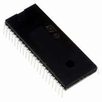
ST72F324J4B6 STMicroelectronics, ST72F324J4B6 Datasheet - Page 136

ST72F324J4B6
Manufacturer Part Number
ST72F324J4B6
Description
IC MCU 8BIT 16K FLASH 42-PDIP
Manufacturer
STMicroelectronics
Series
ST7r
Datasheet
1.ST72F324J2T6.pdf
(164 pages)
Specifications of ST72F324J4B6
Core Processor
ST7
Core Size
8-Bit
Speed
8MHz
Connectivity
SCI, SPI
Peripherals
LVD, POR, PWM, WDT
Number Of I /o
32
Program Memory Size
16KB (16K x 8)
Program Memory Type
FLASH
Ram Size
512 x 8
Voltage - Supply (vcc/vdd)
3.8 V ~ 5.5 V
Data Converters
A/D 12x10b
Oscillator Type
Internal
Operating Temperature
-40°C ~ 85°C
Package / Case
42-DIP (0.600", 15.24mm)
Processor Series
ST72F3x
Core
ST7
Data Bus Width
8 bit
Data Ram Size
512 B
Interface Type
SCI, SPI
Maximum Clock Frequency
8 MHz
Number Of Programmable I/os
32
Number Of Timers
4 bit
Operating Supply Voltage
3.8 V to 5.5 V
Maximum Operating Temperature
+ 85 C
Mounting Style
Through Hole
Development Tools By Supplier
ST7F521-IND/USB, ST7232X-EVAL, ST7MDT20-DVP3, ST7MDT20J-EMU3, STX-RLINK
Minimum Operating Temperature
- 40 C
On-chip Adc
10 bit
For Use With
497-6421 - BOARD EVAL DGTL BATT CHGR DESIGN
Lead Free Status / RoHS Status
Lead free / RoHS Compliant
Eeprom Size
-
Lead Free Status / Rohs Status
Details
Available stocks
Company
Part Number
Manufacturer
Quantity
Price
Part Number:
ST72F324J4B6
Manufacturer:
ST
Quantity:
20 000
ST72324Jx ST72324Kx
12.10 CONTROL PIN CHARACTERISTICS
12.10.1 Asynchronous RESET Pin
Subject to general operating conditions for V
Notes:
1. Data based on characterization results, not tested in production.
2. Hysteresis voltage between Schmitt trigger switching levels.
3. The I
(I/O ports and control pins) must not exceed I
4. To guarantee the reset of the device, a minimum pulse has to be applied to the RESET pin. All short pulses applied on
the RESET pin with a duration below t
5. The reset network (the resistor and two capacitors) protects the device against parasitic resets, especially in noisy en-
vironments.
6. Data guaranteed by design, not tested in production.
136/164
1
t
w(RSTL)out
t
t
Symbol
h(RSTL)in
g(RSTL)in
R
V
V
V
V
I
hys
IO
ON
OL
IH
IL
IO
current sunk must always respect the absolute maximum rating specified in
Schmitt trigger voltage hysteresis
Input low level voltage
Input high level voltage
Output low level voltage
Driving current on RESET pin
Weak pull-up equivalent resistor
Generated reset pulse duration
External reset pulse hold time
Filtered glitch duration
Parameter
1)
5)
1)
3)
h(RSTL)in
4)
VSS
2)
can be ignored.
.
DD
V
V
Internal reset sources
, f
DD
DD
CPU
=5V
=5V
Conditions
, and T
I
IO
=+2mA
A
unless otherwise specified.
0.85xV
Min
2.5
20
20
DD
Section 12.2.2
Typ
2.5
0.2
200
30
30
2
0.16xV
and the sum of I
Max
120
42
0.5
6)
DD
Unit
mA
kΩ
µs
µs
ns
V
V
V
IO


