ST72F521AR9TC STMicroelectronics, ST72F521AR9TC Datasheet - Page 97
ST72F521AR9TC
Manufacturer Part Number
ST72F521AR9TC
Description
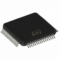
IC MCU 8BIT 60K FLASH 64-TQFP
Manufacturer
STMicroelectronics
Series
ST7r
Datasheet
1.ST72F521M9T6.pdf
(215 pages)
Specifications of ST72F521AR9TC
Core Processor
ST7
Core Size
8-Bit
Speed
8MHz
Connectivity
CAN, I²C, SCI, SPI
Peripherals
LVD, POR, PWM, WDT
Number Of I /o
48
Program Memory Size
60KB (60K x 8)
Program Memory Type
FLASH
Ram Size
2K x 8
Voltage - Supply (vcc/vdd)
3.8 V ~ 5.5 V
Data Converters
A/D 16x10b
Oscillator Type
Internal
Operating Temperature
-40°C ~ 125°C
Package / Case
64-TQFP, 64-VQFP
For Use With
497-6453 - BOARD EVAL BASED ON ST7LNBX
Lead Free Status / RoHS Status
Lead free / RoHS Compliant
Eeprom Size
-
Available stocks
Company
Part Number
Manufacturer
Quantity
Price
Company:

Part Number:
ST72F521AR9TC
Manufacturer:
STMicroelectronics
Quantity:
10 000
Company:
Part Number:
ST72F521AR9TCE
Manufacturer:
STMicroelectronics
Quantity:
10 000
Company:
Part Number:
ST72F521AR9TCTR
Manufacturer:
STMicroelectronics
Quantity:
10 000


SERIAL PERIPHERAL INTERFACE (Cont’d)
10.5.8 Register Description
CONTROL REGISTER (SPICR)
Read/Write
Reset Value: 0000 xxxx (0xh)
Bit 7 = SPIE Serial Peripheral Interrupt Enable.
This bit is set and cleared by software.
0: Interrupt is inhibited
1: An SPI interrupt is generated whenever
Bit 6 = SPE Serial Peripheral Output Enable.
This bit is set and cleared by software. It is also
cleared by hardware when, in master mode, SS=0
(see
(MODF)). The SPE bit is cleared by reset, so the
SPI peripheral is not initially connected to the ex-
ternal pins.
0: I/O pins free for general purpose I/O
1: SPI I/O pin alternate functions enabled
Bit 5 = SPR2 Divider Enable.
This bit is set and cleared by software and is
cleared by reset. It is used with the SPR[1:0] bits to
set the baud rate. Refer to
mode SCK
0: Divider by 2 enabled
1: Divider by 2 disabled
Note: This bit has no effect in slave mode.
Bit 4 = MSTR Master Mode.
This bit is set and cleared by software. It is also
cleared by hardware when, in master mode, SS=0
(see
(MODF)).
0: Slave mode
1: Master mode. The function of the SCK pin
SPIE SPE
SPIF=1, MODF=1 or OVR=1 in the SPICSR
register
changes from an input to an output and the func-
tions of the MISO and MOSI pins are reversed.
7
Section
Section
Frequency.
SPR2
10.5.5.1
10.5.5.1
MSTR
CPOL
Master
Master
Table 18 SPI Master
CPHA
Mode
Mode
SPR1
SPR0
Fault
Fault
0
Bit 3 = CPOL Clock Polarity.
This bit is set and cleared by software. This bit de-
termines the idle state of the serial Clock. The
CPOL bit affects both the master and slave
modes.
0: SCK pin has a low level idle state
1: SCK pin has a high level idle state
Note: If CPOL is changed at the communication
byte boundaries, the SPI must be disabled by re-
setting the SPE bit.
Bit 2 = CPHA Clock Phase.
This bit is set and cleared by software.
0: The first clock transition is the first data capture
1: The second clock transition is the first capture
Note: The slave must have the same CPOL and
CPHA settings as the master.
Bits 1:0 = SPR[1:0] Serial Clock Frequency.
These bits are set and cleared by software. Used
with the SPR2 bit, they select the baud rate of the
SPI serial clock SCK output by the SPI in master
mode.
Note: These 2 bits have no effect in slave mode.
Table 18. SPI Master mode SCK Frequency
edge.
edge.
Serial Clock
f
f
f
f
CPU
f
f
CPU
CPU
CPU
CPU
CPU
/128
/16
/32
/64
/4
/8
SPR2
ST72F521, ST72521B
1
0
0
1
0
0
SPR1
0
0
0
1
1
1
SPR0
97/215
0
0
1
0
0
1
Related parts for ST72F521AR9TC
Image
Part Number
Description
Manufacturer
Datasheet
Request
R

Part Number:
Description:
80/64-PIN 8-BIT MCU WITH 32 TO 60K FLASH/ROM ADC FIVE TIMERS SPI SCI I2C CAN INTERFACE
Manufacturer:
STMicroelectronics
Part Number:
Description:
STMicroelectronics [RIPPLE-CARRY BINARY COUNTER/DIVIDERS]
Manufacturer:
STMicroelectronics
Datasheet:
Part Number:
Description:
STMicroelectronics [LIQUID-CRYSTAL DISPLAY DRIVERS]
Manufacturer:
STMicroelectronics
Datasheet:

Part Number:
Description:
BOARD EVAL FOR MEMS SENSORS
Manufacturer:
STMicroelectronics
Datasheet:
Part Number:
Description:
NPN TRANSISTOR POWER MODULE
Manufacturer:
STMicroelectronics
Datasheet:
Part Number:
Description:
TURBOSWITCH ULTRA-FAST HIGH VOLTAGE DIODE
Manufacturer:
STMicroelectronics
Datasheet:
Part Number:
Description:
Manufacturer:
STMicroelectronics
Datasheet:
Part Number:
Description:
DIODE / SCR MODULE
Manufacturer:
STMicroelectronics
Datasheet:
Part Number:
Description:
DIODE / SCR MODULE
Manufacturer:
STMicroelectronics
Datasheet:
Part Number:
Description:
Search -----> STE16N100
Manufacturer:
STMicroelectronics
Datasheet:
Part Number:
Description:
Search ---> STE53NA50
Manufacturer:
STMicroelectronics
Datasheet:
Part Number:
Description:
NPN Transistor Power Module
Manufacturer:
STMicroelectronics
Datasheet: