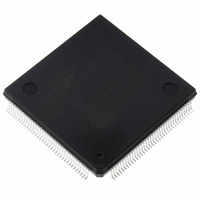
ST10F269Z2Q6 STMicroelectronics, ST10F269Z2Q6 Datasheet - Page 33

ST10F269Z2Q6
Manufacturer Part Number
ST10F269Z2Q6
Description
MCU 16BIT 256K FLASH 144PQFP
Manufacturer
STMicroelectronics
Series
ST10r
Specifications of ST10F269Z2Q6
Core Processor
ST10
Core Size
16-Bit
Speed
40MHz
Connectivity
CAN, EBI/EMI, SSC, UART/USART
Peripherals
POR, PWM, WDT
Number Of I /o
111
Program Memory Size
256KB (256K x 8)
Program Memory Type
FLASH
Ram Size
12K x 8
Voltage - Supply (vcc/vdd)
4.5 V ~ 5.5 V
Data Converters
A/D 16x10b
Oscillator Type
Internal
Operating Temperature
-40°C ~ 85°C
Package / Case
144-QFP
Controller Family/series
ST10
No. Of I/o's
111
Ram Memory Size
12KB
Cpu Speed
40MHz
No. Of Timers
5
Embedded Interface Type
CAN, SSC, USART
Rohs Compliant
Yes
Processor Series
ST10F26x
Core
ST10
Data Bus Width
16 bit
Data Ram Size
12 KB
Interface Type
CAN, SSC, USART
Maximum Clock Frequency
40 MHz
Number Of Programmable I/os
111
Number Of Timers
2 x 16 bit
Operating Supply Voltage
0.3 V to 4 V
Maximum Operating Temperature
+ 85 C
Mounting Style
SMD/SMT
Minimum Operating Temperature
- 40 C
On-chip Adc
16 bit x 10 bit
Lead Free Status / RoHS Status
Lead free / RoHS Compliant
Eeprom Size
-
Lead Free Status / Rohs Status
Details
Other names
497-4833
Available stocks
Company
Part Number
Manufacturer
Quantity
Price
Company:
Part Number:
ST10F269Z2Q6
Manufacturer:
ST
Quantity:
201
Company:
Part Number:
ST10F269Z2Q6
Manufacturer:
ST
Quantity:
745
Company:
Part Number:
ST10F269Z2Q6
Manufacturer:
STMicroelectronics
Quantity:
10 000
Part Number:
ST10F269Z2Q6
Manufacturer:
ST
Quantity:
20 000
ST10F269
Figure 7 : Memory Configuration after Reset
5.6.3 - Loading the Startup Code
After sending the identification Byte the BSL
enters a loop to receive 32 Bytes via ASC0. These
Byte are stored sequentially into locations
00’FA40h through 00’FA5Fh of the internal RAM.
So up to 16 instructions may be placed into the
RAM area. To execute the loaded code the BSL
then jumps to location 00’FA40h, which is the first
loaded instruction.
The
terminated, the ST10F269 remains in BSL mode,
however. Most probably the initially loaded routine
will load additional code or data, as an average
application is likely to require substantially more
than 16 instructions. This second receive loop
may directly use the pre-initialized interface ASC0
to receive
user-defined locations.
This second level of loaded code may be the final
application code. It may also be another, more
sophisticated,
transmission protocol to enhance the integrity of
the loaded code or data. It may also contain a
code
configuration and enable the bus interface to store
the received data into external memory.
This process may go through several iterations or
may directly execute the final application. In all
BSL mode active
EA pin
Code fetch from internal
Flash area
Data fetch from internal
Flash area
bootstrap
sequence
data and
loader
loading
to
routine
Segment
change
Flash
Test
store it to arbitrary
255
2
1
0
sequence
User Flash access
Test-Flash access
Yes (P0L.4=’0’)
IRAM
Flash
16M Bytes
User
that
High
the
Access to:
enabled
internal
adds
is
disabled
Flash
external
system
now
bus
a
Segment
Flash
Test
255
2
1
0
cases the ST10F269 will still run in BSL mode,
that means with the watchdog timer disabled and
limited access to the internal Flash area.
All code fetches from the internal Flash area
(00’0000h...00’7FFFh or 01’0000h...01’7FFFh, if
mapped to segment 1) are redirected to the
special Boot-ROM. Data fetches access will
access the internal Boot-ROM of the ST10F269, if
any is available, but will return undefined data on
ROMless devices.
5.6.4 - Exiting Bootstrap Loader Mode
In order to execute a program in normal mode, the
BSL mode must be terminated first. The
ST10F269 exits BSL mode upon a software reset
(ignores the level on P0L.4) or a hardware reset
(P0L.4 must be high). After a reset the ST10F269
will start executing from location 00’0000h of the
internal Flash or the external memory, as
programmed via pin EA.
User Flash access
Test-Flash access
Yes (P0L.4=’0’)
IRAM
Flash
16M Bytes
User
Low
Access to:
5 - INTERNAL FLASH MEMORY
enabled
internal
Flash
external
enabled
bus
Segment
255
2
1
0
Access to application
User Flash access
User Flash access
IRAM
Flash
User
No (P0L.4=’1’)
16M Bytes
depends on
depends on
Access:
reset config
reset config
EA, Port0
EA, Port0
33/184


