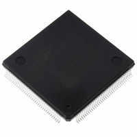
ST10F269Z2Q6 STMicroelectronics, ST10F269Z2Q6 Datasheet - Page 50

ST10F269Z2Q6
Manufacturer Part Number
ST10F269Z2Q6
Description
MCU 16BIT 256K FLASH 144PQFP
Manufacturer
STMicroelectronics
Series
ST10r
Specifications of ST10F269Z2Q6
Core Processor
ST10
Core Size
16-Bit
Speed
40MHz
Connectivity
CAN, EBI/EMI, SSC, UART/USART
Peripherals
POR, PWM, WDT
Number Of I /o
111
Program Memory Size
256KB (256K x 8)
Program Memory Type
FLASH
Ram Size
12K x 8
Voltage - Supply (vcc/vdd)
4.5 V ~ 5.5 V
Data Converters
A/D 16x10b
Oscillator Type
Internal
Operating Temperature
-40°C ~ 85°C
Package / Case
144-QFP
Controller Family/series
ST10
No. Of I/o's
111
Ram Memory Size
12KB
Cpu Speed
40MHz
No. Of Timers
5
Embedded Interface Type
CAN, SSC, USART
Rohs Compliant
Yes
Processor Series
ST10F26x
Core
ST10
Data Bus Width
16 bit
Data Ram Size
12 KB
Interface Type
CAN, SSC, USART
Maximum Clock Frequency
40 MHz
Number Of Programmable I/os
111
Number Of Timers
2 x 16 bit
Operating Supply Voltage
0.3 V to 4 V
Maximum Operating Temperature
+ 85 C
Mounting Style
SMD/SMT
Minimum Operating Temperature
- 40 C
On-chip Adc
16 bit x 10 bit
Lead Free Status / RoHS Status
Lead free / RoHS Compliant
Eeprom Size
-
Lead Free Status / Rohs Status
Details
Other names
497-4833
Available stocks
Company
Part Number
Manufacturer
Quantity
Price
Company:
Part Number:
ST10F269Z2Q6
Manufacturer:
ST
Quantity:
201
Company:
Part Number:
ST10F269Z2Q6
Manufacturer:
ST
Quantity:
745
Company:
Part Number:
ST10F269Z2Q6
Manufacturer:
STMicroelectronics
Quantity:
10 000
Part Number:
ST10F269Z2Q6
Manufacturer:
ST
Quantity:
20 000
9 - CAPTURE/COMPARE (CAPCOM) UNITS
* The CAPCOM2 unit provides 16 capture inputs, but only 12 compare outputs. CC24I to CC27I are inputs only.
Figure 13 : Block Diagram of CAPCOM Timers T0 and T7
Figure 14 : Block Diagram of CAPCOM Timers T1 and T8
Note: When
When a capture/compare register has been
selected for capture mode, the current contents of
the allocated timer will be latched (captured) into
the capture/compare register in response to an
external event at the port pin which is associated
with this register. In addition, a specific interrupt
request for this capture/compare register is
generated.
Either a positive, a negative, or both a positive and
a negative external signal transition at the pin can
be selected as the triggering event. The contents
of all registers which have been selected for one
of the five compare modes are continuously
50/184
TxIN
CPU
Clock
Over / Underflow
GPT2 Timer T6
CPU
Clock
Over / Underflow
GPT2 Timer T6
Pin
connected to the input lines of both T0 and
T7, these timers count the input signal
synchronously. Thus the two timers can be
regarded as one timer whose contents can
be compared with 32 capture registers.
Edge Select
Txl
an
Txl
Txl
X
X
external
MUX
TxM
Txl TxM
Control
Input
MUX
input
TxR
signal
TxR
is
Reload Register TxREL
CAPCOM Timer Tx
compared with the contents of the allocated
timers.
When a match occurs between the timer value
and the value in a capture /compare register,
specific actions will be taken based on the
selected compare mode (see Table 9).
The input frequencies f
selector Tx, are determined as a function of the
CPU
resolution and periods which result from the
selected pre-scaler option in TxI when using a
40MHz CPU clock on PQFP144 devices (or a
32MHz CPU clock on TQFP144 devices) are
listed in Table 10 and Table 11 .
The numbers for the timer periods are based on a
reload value of 0000h. Note that some numbers
may be rounded to 3 significant figures.
Reload Register TxREL
CAPCOM Timer Tx
clocks.
The
timer
Tx
, for the timer input
TxIR
TxIR
input
frequencies,
ST10F269
Interrupt
Request
x = 1, 8
x = 0, 7
Interrupt
Request


