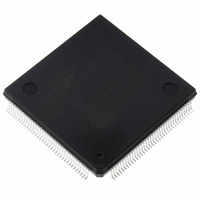
ST10F269Z2Q6 STMicroelectronics, ST10F269Z2Q6 Datasheet - Page 36

ST10F269Z2Q6
Manufacturer Part Number
ST10F269Z2Q6
Description
MCU 16BIT 256K FLASH 144PQFP
Manufacturer
STMicroelectronics
Series
ST10r
Specifications of ST10F269Z2Q6
Core Processor
ST10
Core Size
16-Bit
Speed
40MHz
Connectivity
CAN, EBI/EMI, SSC, UART/USART
Peripherals
POR, PWM, WDT
Number Of I /o
111
Program Memory Size
256KB (256K x 8)
Program Memory Type
FLASH
Ram Size
12K x 8
Voltage - Supply (vcc/vdd)
4.5 V ~ 5.5 V
Data Converters
A/D 16x10b
Oscillator Type
Internal
Operating Temperature
-40°C ~ 85°C
Package / Case
144-QFP
Controller Family/series
ST10
No. Of I/o's
111
Ram Memory Size
12KB
Cpu Speed
40MHz
No. Of Timers
5
Embedded Interface Type
CAN, SSC, USART
Rohs Compliant
Yes
Processor Series
ST10F26x
Core
ST10
Data Bus Width
16 bit
Data Ram Size
12 KB
Interface Type
CAN, SSC, USART
Maximum Clock Frequency
40 MHz
Number Of Programmable I/os
111
Number Of Timers
2 x 16 bit
Operating Supply Voltage
0.3 V to 4 V
Maximum Operating Temperature
+ 85 C
Mounting Style
SMD/SMT
Minimum Operating Temperature
- 40 C
On-chip Adc
16 bit x 10 bit
Lead Free Status / RoHS Status
Lead free / RoHS Compliant
Eeprom Size
-
Lead Free Status / Rohs Status
Details
Other names
497-4833
Available stocks
Company
Part Number
Manufacturer
Quantity
Price
Company:
Part Number:
ST10F269Z2Q6
Manufacturer:
ST
Quantity:
201
Company:
Part Number:
ST10F269Z2Q6
Manufacturer:
ST
Quantity:
745
Company:
Part Number:
ST10F269Z2Q6
Manufacturer:
STMicroelectronics
Quantity:
10 000
Part Number:
ST10F269Z2Q6
Manufacturer:
ST
Quantity:
20 000
6 - CENTRAL PROCESSING UNIT (CPU)
The System Configuration Register SYSCON
This bit-addressable register provides general system configuration and control functions. The reset
value for register SYSCON depends on the state of the PORT0 pins during reset.
SYSCON (FF12h / 89h)
Notes: 1. These bits are set directly or indirectly according to PORT0 and EA pin configuration during reset sequence.
6.1 - Multiplier-accumulator Unit (MAC)
The MAC co-processor is a specialized co-pro-
cessor added to the ST10 CPU Core in order to
improve the performances of the ST10 Family in
signal processing algorithms.
Signal processing needs at least three specialized
units operating in parallel to achieve maximum
performance:
– A Multiply-Accumulate Unit,
– An Address Generation Unit, able to feed the
– A Repeat Unit, to execute series of multiply-ac-
36/184
XPEN
BDRSTEN
OWDDIS
PWDCFG
CSCFG
15
MAC Unit with 2 operands per cycle,
cumulate instructions.
Bit
2. Register SYSCON cannot be changed after execution of the EINIT instruction.
STKSZ
RW
14
0
1
0
1
0
1
0
1
0
1
13
XBUS Peripheral Enable Bit
Accesses to the on-chip X-Peripherals and their functions are disabled
The on-chip X-Peripherals are enabled and can be accessed.
Bidirectional Reset Enable
RSTIN pin is an input pin only. SW Reset or WDT Reset have no effect on this pin
RSTIN pin is a bidirectional pin. This pin is pulled low during 1024 TCL during reset sequence.
Oscillator Watchdog Disable Control
Oscillator Watchdog (OWD) is enabled. If PLL is bypassed, the OWD monitors XTAL1 activity. If
there is no activity on XTAL1 for at least 1 s, the CPU clock is switched automatically to PLL’s
base frequency (2 to 10MHz).
OWD is disabled. If the PLL is bypassed, the CPU clock is always driven by XTAL1 signal. The PLL
is turned off to reduce power supply current.
Power Down Mode Configuration Control
Power Down Mode can only be entered during PWRDN instruction execution if NMI pin is low, oth-
erwise the instruction has no effect. To exit Power Down Mode, an external reset must occurs by
asserting the RSTIN pin.
Power Down Mode can only be entered during PWRDN instruction execution if all enabled fast
external interrupt EXxIN pins are in their inactive level. Exiting this mode can be done by asserting
one enabled EXxIN pin.
Chip Select Configuration Control
Latched Chip Select lines: CSx change 1 TCL after rising edge of ALE
Unlatched Chip Select lines: CSx change with rising edge of ALE
ROM
RW
12
S1
SGT
RW
DIS
11
RW
ROM
10
EN
1
RW
BYT
DIS
9
1
CLK
RW
EN
8
SFR
RW
CFG
WR
Function
The existing ST10 CPU has been modified to
include new addressing capabilities which enable
the CPU to supply the new co-processor with up
to 2 operands per instruction cycle.
This new co-processor (so-called MAC) contains
a fast multiply-accumulate unit and a repeat unit.
The co-processor instructions extend the ST10
CPU instruction set with multiply, multiply-accu-
mulate, 32-bit signed arithmetic operations.
A new transfer instruction CoMOV has also been
added to take benefit of the new addressing capa-
bilities.
7
1
CFG
RW
CS
6
PWD
CFG
RW
5
OWD
RW
DIS
4
STEN
BDR
RW
3
Reset Value: 0xx0h
XPEN
RW
2
ST10F269
VISI
BLE
RW
1
SHARE
XPER-
RW
0


