C8051F333-GMR Silicon Laboratories Inc, C8051F333-GMR Datasheet - Page 4
C8051F333-GMR
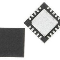
Manufacturer Part Number
C8051F333-GMR
Description
IC 8051 MCU 4K FLASH 20MLP
Manufacturer
Silicon Laboratories Inc
Series
C8051F33xr
Specifications of C8051F333-GMR
Core Processor
8051
Core Size
8-Bit
Speed
25MHz
Connectivity
SMBus (2-Wire/I²C), SPI, UART/USART
Peripherals
POR, PWM, WDT
Number Of I /o
17
Program Memory Size
4KB (4K x 8)
Program Memory Type
FLASH
Ram Size
768 x 8
Voltage - Supply (vcc/vdd)
2.7 V ~ 3.6 V
Oscillator Type
Internal
Operating Temperature
-40°C ~ 85°C
Package / Case
20-QFN
Processor Series
C8051F3x
Core
8051
Data Bus Width
8 bit
Data Ram Size
768 B
Interface Type
I2C, SPI, UART
Maximum Clock Frequency
25 MHz
Number Of Programmable I/os
17
Number Of Timers
4
Operating Supply Voltage
2.7 V to 3.6 V
Maximum Operating Temperature
+ 85 C
Mounting Style
SMD/SMT
3rd Party Development Tools
KSK-SL-TOOLSTICK, PK51, CA51, A51, ULINK2
Development Tools By Supplier
C8051F330DK
Minimum Operating Temperature
- 40 C
For Use With
336-1451 - ADAPTER PROGRAM TOOLSTICK F330
Lead Free Status / RoHS Status
Lead free / RoHS Compliant
Eeprom Size
-
Data Converters
-
Lead Free Status / Rohs Status
Details
Available stocks
Company
Part Number
Manufacturer
Quantity
Price

Part Number:
C8051F333-GMR
Manufacturer:
SILICON LABS/èٹ¯ç§‘
Quantity:
20 000


C8051F330/1/2/3/4/5
10. Reset Sources......................................................................................................... 97
11. Flash Memory ....................................................................................................... 103
12. External RAM ........................................................................................................ 111
13. Oscillators ............................................................................................................. 113
14. Port Input/Output.................................................................................................. 123
4
9.3. Interrupt Handler ............................................................................................... 85
9.4. Power Management Modes .............................................................................. 94
10.1.Power-On Reset ............................................................................................... 98
10.2.Power-Fail Reset/VDD Monitor ........................................................................ 98
10.3.External Reset .................................................................................................. 99
10.4.Missing Clock Detector Reset .......................................................................... 99
10.5.Comparator0 Reset ........................................................................................ 100
10.6.PCA Watchdog Timer Reset .......................................................................... 100
10.7.Flash Error Reset ........................................................................................... 100
10.8.Software Reset ............................................................................................... 100
11.1.Programming The Flash Memory ................................................................... 103
11.2.Non-volatile Data Storage .............................................................................. 104
11.3.Security Options ............................................................................................. 105
11.4.Flash Write and Erase Guidelines .................................................................. 107
13.1.Programmable Internal High-Frequency (H-F) Oscillator ............................... 113
13.2.Programmable Internal Low-Frequency (L-F) Oscillator ................................ 115
13.3.External Oscillator Drive Circuit...................................................................... 116
13.4.System Clock Selection.................................................................................. 121
14.1.Priority Crossbar Decoder .............................................................................. 125
14.2.Port I/O Initialization ....................................................................................... 127
9.2.5. Stack ....................................................................................................... 78
9.2.6. Special Function Registers....................................................................... 79
9.2.7. Register Descriptions ............................................................................... 83
9.3.1. MCU Interrupt Sources and Vectors ........................................................ 86
9.3.2. External Interrupts .................................................................................... 87
9.3.3. Interrupt Priorities ..................................................................................... 87
9.3.4. Interrupt Latency ...................................................................................... 87
9.3.5. Interrupt Register Descriptions................................................................. 89
9.4.1. Idle Mode.................................................................................................. 94
9.4.2. Stop Mode ................................................................................................ 95
11.1.1.Flash Lock and Key Functions ............................................................... 103
11.1.2.Flash Erase Procedure .......................................................................... 103
11.1.3.Flash Write Procedure ........................................................................... 104
11.4.1.V
11.4.2.PSWE Maintenance ............................................................................... 107
11.4.3.System Clock ......................................................................................... 108
13.2.1.Calibrating the Internal L-F Oscillator..................................................... 115
13.3.1.External Crystal Example....................................................................... 118
13.3.2.External RC Example............................................................................. 120
13.3.3.External Capacitor Example................................................................... 120
DD
Maintenance and the V
Rev. 1.7
DD
monitor ................................................. 107
Related parts for C8051F333-GMR
Image
Part Number
Description
Manufacturer
Datasheet
Request
R

Part Number:
Description:
SMD/C°/SINGLE-ENDED OUTPUT SILICON OSCILLATOR
Manufacturer:
Silicon Laboratories Inc
Part Number:
Description:
Manufacturer:
Silicon Laboratories Inc
Datasheet:
Part Number:
Description:
N/A N/A/SI4010 AES KEYFOB DEMO WITH LCD RX
Manufacturer:
Silicon Laboratories Inc
Datasheet:
Part Number:
Description:
N/A N/A/SI4010 SIMPLIFIED KEY FOB DEMO WITH LED RX
Manufacturer:
Silicon Laboratories Inc
Datasheet:
Part Number:
Description:
N/A/-40 TO 85 OC/EZLINK MODULE; F930/4432 HIGH BAND (REV E/B1)
Manufacturer:
Silicon Laboratories Inc
Part Number:
Description:
EZLink Module; F930/4432 Low Band (rev e/B1)
Manufacturer:
Silicon Laboratories Inc
Part Number:
Description:
I°/4460 10 DBM RADIO TEST CARD 434 MHZ
Manufacturer:
Silicon Laboratories Inc
Part Number:
Description:
I°/4461 14 DBM RADIO TEST CARD 868 MHZ
Manufacturer:
Silicon Laboratories Inc
Part Number:
Description:
I°/4463 20 DBM RFSWITCH RADIO TEST CARD 460 MHZ
Manufacturer:
Silicon Laboratories Inc
Part Number:
Description:
I°/4463 20 DBM RADIO TEST CARD 868 MHZ
Manufacturer:
Silicon Laboratories Inc
Part Number:
Description:
I°/4463 27 DBM RADIO TEST CARD 868 MHZ
Manufacturer:
Silicon Laboratories Inc
Part Number:
Description:
I°/4463 SKYWORKS 30 DBM RADIO TEST CARD 915 MHZ
Manufacturer:
Silicon Laboratories Inc
Part Number:
Description:
N/A N/A/-40 TO 85 OC/4463 RFMD 30 DBM RADIO TEST CARD 915 MHZ
Manufacturer:
Silicon Laboratories Inc
Part Number:
Description:
I°/4463 20 DBM RADIO TEST CARD 169 MHZ
Manufacturer:
Silicon Laboratories Inc