TMP86FH46ANG(Z) Toshiba, TMP86FH46ANG(Z) Datasheet - Page 12
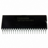
TMP86FH46ANG(Z)
Manufacturer Part Number
TMP86FH46ANG(Z)
Description
IC MCU 8BIT FLASH 16KB 42-SDIP
Manufacturer
Toshiba
Series
TLCS-870/Cr
Datasheet
1.TMP86FH46ANGZ.pdf
(214 pages)
Specifications of TMP86FH46ANG(Z)
Core Processor
870/C
Core Size
8-Bit
Speed
16MHz
Connectivity
SIO, UART/USART
Peripherals
LED, PWM, WDT
Number Of I /o
33
Program Memory Size
16KB (16K x 8)
Program Memory Type
FLASH
Ram Size
512 x 8
Voltage - Supply (vcc/vdd)
2.7 V ~ 5.5 V
Data Converters
A/D 8x10b
Oscillator Type
Internal
Operating Temperature
-40°C ~ 85°C
Package / Case
42-SDIP (0.600", 15.24mm)
Processor Series
TLCS-870
Core
870/C
Data Bus Width
8 bit
Data Ram Size
512 B
Interface Type
SIO, UART
Maximum Clock Frequency
16 MHz
Number Of Programmable I/os
33
Number Of Timers
3
Maximum Operating Temperature
+ 85 C
Mounting Style
Through Hole
Development Tools By Supplier
BMSKTOPAS86FH47(AND), BM1040R0A, BMP86A100010A, BMP86A100010B, BMP86A200010B, BMP86A200020A, BMP86A300010A, BMP86A300020A, BMP86A300030A, SW89CN0-ZCC, SW00MN0-ZCC
Minimum Operating Temperature
- 40 C
On-chip Adc
10 bit, 8 Channel
For Use With
BM1401W0A-G - FLASH WRITER ON-BOARD PROGRAMTMP86C909XB - EMULATION CHIP FOR TMP86F SDIP
Lead Free Status / RoHS Status
Lead free / RoHS Compliant
Eeprom Size
-
Lead Free Status / Rohs Status
Details
Other names
TMP86FH46ANGZ


12. 10-bit AD Converter (ADC)
13. Key-on Wakeup (KWU)
14. Flash Memory
15. Serial PROM Mode
iv
11.9
12.1
12.2
12.3
12.4
12.5
12.6
13.1
13.2
13.3
14.1
14.2
14.3
14.4
15.1
11.9.1
11.9.2
11.9.3
11.9.4
11.9.5
11.9.6
12.3.1
12.3.2
12.3.3
12.6.1
12.6.2
12.6.3
14.1.1
14.1.1
14.1.2
14.2.1
14.2.2
14.2.3
14.2.4
14.2.5
14.2.6
14.4.1
14.4.2
14.4.1.1
14.4.2.1
Status Flag . . . . . . . . . . . . . . . . . . . . . . . . . . . . . . . . . . . . . . . . . . . . . . . . . . . . 127
Configuration . . . . . . . . . . . . . . . . . . . . . . . . . . . . . . . . . . . . . . . . . . . . . . . . . . 131
Register configuration . . . . . . . . . . . . . . . . . . . . . . . . . . . . . . . . . . . . . . . . . . . . 132
STOP/SLOW Modes during AD Conversion . . . . . . . . . . . . . . . . . . . . . . . . . . . 137
Analog Input Voltage and AD Conversion Result . . . . . . . . . . . . . . . . . . . . . . . 138
Precautions about AD Converter . . . . . . . . . . . . . . . . . . . . . . . . . . . . . . . . . . . . 139
Configuration . . . . . . . . . . . . . . . . . . . . . . . . . . . . . . . . . . . . . . . . . . . . . . . . . . . 141
Control . . . . . . . . . . . . . . . . . . . . . . . . . . . . . . . . . . . . . . . . . . . . . . . . . . . . . . . . 141
Function . . . . . . . . . . . . . . . . . . . . . . . . . . . . . . . . . . . . . . . . . . . . . . . . . . . . . . . 141
Flash Memory Control . . . . . . . . . . . . . . . . . . . . . . . . . . . . . . . . . . . . . . . . . . . . 144
Command Sequence . . . . . . . . . . . . . . . . . . . . . . . . . . . . . . . . . . . . . . . . . . . . . 146
Toggle Bit (D6) . . . . . . . . . . . . . . . . . . . . . . . . . . . . . . . . . . . . . . . . . . . . . . . . . 148
Access to the Flash Memory Area. . . . . . . . . . . . . . . . . . . . . . . . . . . . . . . . . . . 149
Outline . . . . . . . . . . . . . . . . . . . . . . . . . . . . . . . . . . . . . . . . . . . . . . . . . . . . . . . . 153
Function. . . . . . . . . . . . . . . . . . . . . . . . . . . . . . . . . . . . . . . . . . . . . . . . . . . . . . 135
Parity Error.......................................................................................................................................... 127
Framing Error...................................................................................................................................... 127
Overrun Error ...................................................................................................................................... 127
Receive Data Buffer Full..................................................................................................................... 128
Transmit Data Buffer Empty ............................................................................................................... 128
Transmit End Flag .............................................................................................................................. 129
Software Start Mode ........................................................................................................................... 135
Repeat Mode ...................................................................................................................................... 135
Analog input pin voltage range ........................................................................................................... 139
Analog input shared pins .................................................................................................................... 139
Noise Countermeasure ....................................................................................................................... 139
Flash Memory Command Sequence Execution Control (FLSCR<FLSMD>) ..................................... 144
Flash Memory Standby Control (FLSSTB<FSTB>) ............................................................................ 144
Byte Program ...................................................................................................................................... 146
Sector Erase (4-kbyte Erase) ............................................................................................................. 146
Chip Erase (All Erase) ........................................................................................................................ 147
Product ID Entry ................................................................................................................................. 147
Product ID Exit .................................................................................................................................... 147
Read Protect ....................................................................................................................................... 147
Flash Memory Control in the Serial PROM Mode............................................................................... 149
Flash Memory Control in the MCU mode............................................................................................ 151
............................................................................................................................................................ 144
Register Setting ................................................................................................................................ 136
How to write to the flash memory by executing the control program in the RAM area (in the RAM loader mode within the
How to write to the flash memory by executing a user write control program in the RAM area (in the MCU mode)
serial PROM mode)
Related parts for TMP86FH46ANG(Z)
Image
Part Number
Description
Manufacturer
Datasheet
Request
R

Part Number:
Description:
Toshiba Semiconductor [TOSHIBA IGBT Module Silicon N Channel IGBT]
Manufacturer:
TOSHIBA Semiconductor CORPORATION
Datasheet:
Part Number:
Description:
TOSHIBA GTR MODULE SILICON NPN TRIPLE DIFFUSED TYPE
Manufacturer:
TOSHIBA Semiconductor CORPORATION
Datasheet:
Part Number:
Description:
TOSHIBA GTR Module Silicon N Channel IGBT
Manufacturer:
TOSHIBA Semiconductor CORPORATION
Datasheet:
Part Number:
Description:
TOSHIBA Intelligent Power Module Silicon N Channel IGBT
Manufacturer:
TOSHIBA Semiconductor CORPORATION
Datasheet:
Part Number:
Description:
TOSHIBA INTELLIGENT POWER MODULE SILICON N CHANNEL LGBT
Manufacturer:
TOSHIBA Semiconductor CORPORATION
Datasheet:
Part Number:
Description:
TOSHIBA IGBT Module Silicon N Channel IGBT
Manufacturer:
TOSHIBA Semiconductor CORPORATION
Datasheet:
Part Number:
Description:
TOSHIBA GTR MODULE SILICON N−CHANNEL IGBT
Manufacturer:
TOSHIBA Semiconductor CORPORATION
Datasheet:
Part Number:
Description:
TOSHIBA Intelligent Power Module Silicon N Channel IGBT
Manufacturer:
TOSHIBA Semiconductor CORPORATION
Datasheet:
Part Number:
Description:
TOSHIBA GTR Module Silicon N Channel IGBT
Manufacturer:
TOSHIBA Semiconductor CORPORATION
Datasheet:
Part Number:
Description:
TOSHIBA INTELLIGENT POWER MODULE
Manufacturer:
TOSHIBA Semiconductor CORPORATION
Datasheet:
Part Number:
Description:
TOSHIBA Intelligent Power Module Silicon N Channel IGBT
Manufacturer:
TOSHIBA Semiconductor CORPORATION
Datasheet:
Part Number:
Description:
TOSHIBA Intelligent Power Module Silicon N Channel IGBT
Manufacturer:
TOSHIBA Semiconductor CORPORATION
Datasheet:
Part Number:
Description:
TOSHIBA IGBT Module Silicon N Channel IGBT
Manufacturer:
TOSHIBA Semiconductor CORPORATION
Datasheet:
Part Number:
Description:
TOSHIBA Intelligent Power Module Silicon N Channel IGBT
Manufacturer:
TOSHIBA Semiconductor CORPORATION
Datasheet:
Part Number:
Description:
Toshiba Semiconductor [SILICON N CHANNEL 1GBT]
Manufacturer:
TOSHIBA Semiconductor CORPORATION
Datasheet: