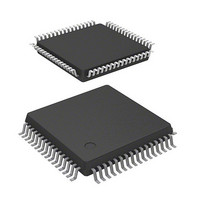
HD64F3687GFP Renesas Electronics America, HD64F3687GFP Datasheet - Page 26

HD64F3687GFP
Manufacturer Part Number
HD64F3687GFP
Description
IC H8 MCU FLASH 56K 64-LQFP
Manufacturer
Renesas Electronics America
Series
H8® H8/300H Tinyr
Datasheet
1.HD64F3684GFPV.pdf
(538 pages)
Specifications of HD64F3687GFP
Core Processor
H8/300H
Core Size
16-Bit
Speed
20MHz
Connectivity
I²C, SCI
Peripherals
LVD, POR, PWM, WDT
Number Of I /o
45
Program Memory Size
56KB (56K x 8)
Program Memory Type
FLASH
Ram Size
4K x 8
Voltage - Supply (vcc/vdd)
3 V ~ 5.5 V
Data Converters
A/D 8x10b
Oscillator Type
Internal
Operating Temperature
-20°C ~ 75°C
Package / Case
64-LQFP
Lead Free Status / RoHS Status
Contains lead / RoHS non-compliant
Eeprom Size
-
Available stocks
Company
Part Number
Manufacturer
Quantity
Price
Company:
Part Number:
HD64F3687GFP
Manufacturer:
Renesas Electronics America
Quantity:
10 000
Company:
Part Number:
HD64F3687GFPMV
Manufacturer:
Renesas Electronics America
Quantity:
10 000
Company:
Part Number:
HD64F3687GFPV
Manufacturer:
Renesas Electronics America
Quantity:
10 000
- Current page: 26 of 538
- Download datasheet (4Mb)
Figure 13.27 Example of Reset Synchronous PWM Mode Operation (OLS0 = OLS1 = 1) ...... 219
Figure 13.28 Example of Reset Synchronous PWM Mode Operation (OLS0 = OLS1 = 0) ...... 220
Figure 13.29 Example of Complementar y PWM Mode Setting Procedure............................... 222
Figure 13.30 Canceling Procedure of Complementary PWM Mode.......................................... 223
Figure 13.31 Example of Complementary PWM Mode Operation (1) ...................................... 224
Figure 13.32 (1) Example of Complementary PWM Mode Operation
Figure 13.32 (2) Example of Complementary PWM Mode Operation
Figure 13.33 Timing of Overshooting ........................................................................................ 227
Figure 13.34 Timing of Undershooting ...................................................................................... 227
Figure 13.35 Compare Match Buffer Operation......................................................................... 230
Figure 13.36 Input Capture Buffer Operation............................................................................. 231
Figure 13.37 Example of Buffer Operation Setting Procedure................................................... 231
Figure 13.38 Example of Buffer Operation (1)
Figure 13.39 Example of Compare Match Timing for Buffer Operation ................................... 233
Figure 13.40 Example of Buffer Operation (2)
Figure 13.41 Input Capture Timing of Buffer Operation............................................................ 235
Figure 13.42 Buffer Operation (3) (Buffer Operation in Complementary
Figure 13.43 Buffer Operation (4) (Buffer Operation in
Figure 13.44 Example of Output Disable Timing of Timer Z by Writing to TOER .................. 238
Figure 13.45 Example of Output Disable Timing of Timer Z by External Trigger.................... 238
Figure 13.46 Example of Output Inverse Timing of Timer Z by Writing to TFCR ................... 239
Figure 13.47 Example of Output Inverse Timing of Timer Z by Writing to POCR................... 239
Figure 13.48 IMF Flag Set Timing when Compare Match Occurs ............................................ 240
Figure 13.49 IMF Flag Set Timing at Input Capture .................................................................. 241
Figure 13.50 OVF Flag Set Timing ............................................................................................ 241
Figure 13.51 Status Flag Clearing Timing.................................................................................. 242
Figure 13.52 Contention between TCNT Write and Clear Operations....................................... 242
Figure 13.53 Contention between TCNT Write and Increment Operations ............................... 243
Figure 13.54 Contention between GR Write and Compare Match............................................. 244
Figure 13.55 Contention between TCNT Write and Overflow................................................... 245
Figure 13.56 Contention between GR Read and Input Capture.................................................. 246
Figure 13.57 Contention between Count Clearing and Increment
Figure 13.58 Contention between GR Write and Input Capture................................................. 248
Rev.5.00 Nov. 02, 2005 Page xxiv of xxxii
(Buffer Operation for Output Compare Register) ................................................. 232
(Buffer Operation for Input Capture Register) ...................................................... 234
PWM Mode CMD1 = CMD0 = 1) ........................................................................ 236
Complementary PWM Mode CMD1 = CMD0 = 1).............................................. 237
Operations by Input Capture ................................................................................ 247
(TPSC2 = TPSC1 = TPSC0 = 0) (2) ................................................................ 225
(TPSC2 = TPSC1 = TPSC0 0) (3) ................................................................ 226
Related parts for HD64F3687GFP
Image
Part Number
Description
Manufacturer
Datasheet
Request
R

Part Number:
Description:
KIT STARTER FOR M16C/29
Manufacturer:
Renesas Electronics America
Datasheet:

Part Number:
Description:
KIT STARTER FOR R8C/2D
Manufacturer:
Renesas Electronics America
Datasheet:

Part Number:
Description:
R0K33062P STARTER KIT
Manufacturer:
Renesas Electronics America
Datasheet:

Part Number:
Description:
KIT STARTER FOR R8C/23 E8A
Manufacturer:
Renesas Electronics America
Datasheet:

Part Number:
Description:
KIT STARTER FOR R8C/25
Manufacturer:
Renesas Electronics America
Datasheet:

Part Number:
Description:
KIT STARTER H8S2456 SHARPE DSPLY
Manufacturer:
Renesas Electronics America
Datasheet:

Part Number:
Description:
KIT STARTER FOR R8C38C
Manufacturer:
Renesas Electronics America
Datasheet:

Part Number:
Description:
KIT STARTER FOR R8C35C
Manufacturer:
Renesas Electronics America
Datasheet:

Part Number:
Description:
KIT STARTER FOR R8CL3AC+LCD APPS
Manufacturer:
Renesas Electronics America
Datasheet:

Part Number:
Description:
KIT STARTER FOR RX610
Manufacturer:
Renesas Electronics America
Datasheet:

Part Number:
Description:
KIT STARTER FOR R32C/118
Manufacturer:
Renesas Electronics America
Datasheet:

Part Number:
Description:
KIT DEV RSK-R8C/26-29
Manufacturer:
Renesas Electronics America
Datasheet:

Part Number:
Description:
KIT STARTER FOR SH7124
Manufacturer:
Renesas Electronics America
Datasheet:

Part Number:
Description:
KIT STARTER FOR H8SX/1622
Manufacturer:
Renesas Electronics America
Datasheet:


