DF2212CUNP24V Renesas Electronics America, DF2212CUNP24V Datasheet - Page 443
DF2212CUNP24V
Manufacturer Part Number
DF2212CUNP24V
Description
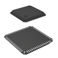
MCU 16BIT FLASH 3V 128K 64-QFN
Manufacturer
Renesas Electronics America
Series
H8® H8S/2200r
Datasheet
1.DF2218UTF24V.pdf
(758 pages)
Specifications of DF2212CUNP24V
Core Processor
H8S/2000
Core Size
16-Bit
Speed
24MHz
Connectivity
SCI, SmartCard, USB
Peripherals
DMA, POR, PWM, WDT
Number Of I /o
37
Program Memory Size
128KB (128K x 8)
Program Memory Type
FLASH
Ram Size
12K x 8
Voltage - Supply (vcc/vdd)
2.7 V ~ 3.6 V
Data Converters
A/D 6x10b
Oscillator Type
External
Operating Temperature
-20°C ~ 75°C
Package / Case
64-QFN
Lead Free Status / RoHS Status
Lead free / RoHS Compliant
Eeprom Size
-
Available stocks
Company
Part Number
Manufacturer
Quantity
Price
Company:

Part Number:
DF2212CUNP24V
Manufacturer:
Renesas Electronics America
Quantity:
135


Bit
7
6 to
4
3
2
1
0
Bit Name Initial Value
ACS3
—
TIOCA2E 1
TIOCA1E 1
TIOCC0E 1
TIOCA0E 1
0
Undefined
R/W
R/W
—
R/W
R/W
R/W
R/W
Selects the clock source in asynchronous mode
depending on the combination with the ACS2 to ACS0
(bits 2 to 0 in SEMRA_0). For details, see section 12.3.9,
Serial Extended Mode Register A_0 (SEMRA_0).
Reserved
The write value should always be 0.
TIOCA2 Output Enable
Controls the TIOCA2 output on the P16 pin.
When the TIOCA2 in TPU is output to generate the
transfer clock, P16 is used as other function pin by
setting this bit to 0.
0: Disables output of TIOCA2 in TPU
1: Enables output of TIOCA2 in TPU
TIOCA1 Output Enable
Controls the TIOCA1 output on the P14 pin.
When the TIOCA1 in TPU is output to generate the
transfer clock, P14 is used as other function pin by
setting this bit to 0.
0: Disables output of TIOCA1 in TPU
1: Enables output TIOCA1 in TPU
Controls the TIOCC0 output on the P12 pin.
When the TIOCC0 in TPU is output to generate the
transfer clock, P12 is used as other function pin by
setting this bit to 0.
0: Disables output of TIOCC0 in TPU
1: Enables output of TIOCC0 in TPU
TIOCA0 Output Enable
Controls the TIOCA0 output on the P10 pin.
When the TIOCA0 in TPU is output to generate the
transfer clock, P10 is used as other function pin by
setting this bit to 0.
0: Disables output of TIOCA0 in TPU
1: Enables output of TIOCA0 in TPU
Description
Asynchronous Clock Source Select
TIOCC0 Output Enable
Rev.7.00 Dec. 24, 2008 Page 387 of 698
REJ09B0074-0700
Related parts for DF2212CUNP24V
Image
Part Number
Description
Manufacturer
Datasheet
Request
R

Part Number:
Description:
KIT STARTER FOR M16C/29
Manufacturer:
Renesas Electronics America
Datasheet:

Part Number:
Description:
KIT STARTER FOR R8C/2D
Manufacturer:
Renesas Electronics America
Datasheet:

Part Number:
Description:
R0K33062P STARTER KIT
Manufacturer:
Renesas Electronics America
Datasheet:

Part Number:
Description:
KIT STARTER FOR R8C/23 E8A
Manufacturer:
Renesas Electronics America
Datasheet:

Part Number:
Description:
KIT STARTER FOR R8C/25
Manufacturer:
Renesas Electronics America
Datasheet:

Part Number:
Description:
KIT STARTER H8S2456 SHARPE DSPLY
Manufacturer:
Renesas Electronics America
Datasheet:

Part Number:
Description:
KIT STARTER FOR R8C38C
Manufacturer:
Renesas Electronics America
Datasheet:

Part Number:
Description:
KIT STARTER FOR R8C35C
Manufacturer:
Renesas Electronics America
Datasheet:

Part Number:
Description:
KIT STARTER FOR R8CL3AC+LCD APPS
Manufacturer:
Renesas Electronics America
Datasheet:
Part Number:
Description:
KIT STARTER FOR RX610
Manufacturer:
Renesas Electronics America
Datasheet:

Part Number:
Description:
KIT STARTER FOR R32C/118
Manufacturer:
Renesas Electronics America
Datasheet:

Part Number:
Description:
KIT DEV RSK-R8C/26-29
Manufacturer:
Renesas Electronics America
Datasheet:

Part Number:
Description:
KIT STARTER FOR SH7124
Manufacturer:
Renesas Electronics America
Datasheet:

Part Number:
Description:
KIT STARTER FOR H8SX/1622
Manufacturer:
Renesas Electronics America
Datasheet:

Part Number:
Description:
KIT DEV FOR SH7203
Manufacturer:
Renesas Electronics America
Datasheet: