DF2212CUNP24V Renesas Electronics America, DF2212CUNP24V Datasheet - Page 509
DF2212CUNP24V
Manufacturer Part Number
DF2212CUNP24V
Description
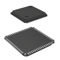
MCU 16BIT FLASH 3V 128K 64-QFN
Manufacturer
Renesas Electronics America
Series
H8® H8S/2200r
Datasheet
1.DF2218UTF24V.pdf
(758 pages)
Specifications of DF2212CUNP24V
Core Processor
H8S/2000
Core Size
16-Bit
Speed
24MHz
Connectivity
SCI, SmartCard, USB
Peripherals
DMA, POR, PWM, WDT
Number Of I /o
37
Program Memory Size
128KB (128K x 8)
Program Memory Type
FLASH
Ram Size
12K x 8
Voltage - Supply (vcc/vdd)
2.7 V ~ 3.6 V
Data Converters
A/D 6x10b
Oscillator Type
External
Operating Temperature
-20°C ~ 75°C
Package / Case
64-QFN
Lead Free Status / RoHS Status
Lead free / RoHS Compliant
Eeprom Size
-
Available stocks
Company
Part Number
Manufacturer
Quantity
Price
Company:

Part Number:
DF2212CUNP24V
Manufacturer:
Renesas Electronics America
Quantity:
135


Section 13 Boundary Scan Function
EXTEST: The EXTEST instruction is used to test external circuits when this LSI is installed on
the print circuit board. If this instruction is executed, output pins are used to output test data
(specified by the SAMPLE/PRELOAD instruction) from the boundary scan register to the print
circuit board, and input pins are used to input test results.
SAMPLE/PRELOAD: The SAMPLE/PRELOAD instruction is used to input data from the LSI
internal circuits to the boundary scan register, output data from scan path, and reload the data to
the scan path. While this instruction is executed, input signals are directly input to the LSI and
output signals are also directly output to the external circuits. The LSI system circuit is not
affected by this instruction.
In SAMPLE operation, the boundary scan register latches the snap shot of data transferred from
input pins to internal circuit or data transferred from internal circuit to output pins. The latched
data is read from the scan path. The scan register latches the snap data at the rising edge of the
TCK in Capture-DR state. The scan register latches snap shot without affecting the LSI normal
operation.
In PRELOAD operation, initial value is written from the scan path to the parallel output latch of
the boundary scan register prior to the EXTEST instruction execution. If the EXTEST is executed
without executing this RELOAD operation, undefined values are output from the beginning to the
end (transfer to the output latch) of the EXTEST sequence. (In EXTEST instruction, output
parallel latches are always output to the output pins.)
CLAMP: When the CLAMP instruction is selected output pins output the boundary scan register
value which was specified by the SAMPLE/PRELOAD instruction in advance. While the CLAMP
instruction is selected, the status of boundary scan register is maintained regardless of the TAP
controller state. BYPASS is connected between TDI and TDO, the same operation as BYPASS
instruction can be achieved.
HIGHZ: When the HIGHZ instruction is selected, all outputs enter high-impedance state. While
this instruction is selected, the status of boundary scan register is maintained regardless of the TAP
controller state. BYPASS resistor is connected between TDI and TDO, the same operation as
BYPASS instruction can be achieved.
IDCODE: When the IDCODE instruction is selected, IDCODE register value is output to the
TDO in Shift-DR state of TAP controller. In this case, IDCODE register value is output from the
LSB. During this instruction execution, test circuit does not affect the system circuit. INSTR is
initialized by the IDCODE instruction in Test-Logic-Reset state of TAP controller.
BYPASS: The BYPASS instruction is a standard instruction necessary to operate bypass register.
The BYPASS instruction improves the serial data transfer speed by bypassing the scan path.
During this instruction execution, test circuit does not affect the system circuit.
Rev.7.00 Dec. 24, 2008 Page 453 of 698
REJ09B0074-0700
Related parts for DF2212CUNP24V
Image
Part Number
Description
Manufacturer
Datasheet
Request
R

Part Number:
Description:
KIT STARTER FOR M16C/29
Manufacturer:
Renesas Electronics America
Datasheet:

Part Number:
Description:
KIT STARTER FOR R8C/2D
Manufacturer:
Renesas Electronics America
Datasheet:

Part Number:
Description:
R0K33062P STARTER KIT
Manufacturer:
Renesas Electronics America
Datasheet:

Part Number:
Description:
KIT STARTER FOR R8C/23 E8A
Manufacturer:
Renesas Electronics America
Datasheet:

Part Number:
Description:
KIT STARTER FOR R8C/25
Manufacturer:
Renesas Electronics America
Datasheet:

Part Number:
Description:
KIT STARTER H8S2456 SHARPE DSPLY
Manufacturer:
Renesas Electronics America
Datasheet:

Part Number:
Description:
KIT STARTER FOR R8C38C
Manufacturer:
Renesas Electronics America
Datasheet:

Part Number:
Description:
KIT STARTER FOR R8C35C
Manufacturer:
Renesas Electronics America
Datasheet:

Part Number:
Description:
KIT STARTER FOR R8CL3AC+LCD APPS
Manufacturer:
Renesas Electronics America
Datasheet:
Part Number:
Description:
KIT STARTER FOR RX610
Manufacturer:
Renesas Electronics America
Datasheet:

Part Number:
Description:
KIT STARTER FOR R32C/118
Manufacturer:
Renesas Electronics America
Datasheet:

Part Number:
Description:
KIT DEV RSK-R8C/26-29
Manufacturer:
Renesas Electronics America
Datasheet:

Part Number:
Description:
KIT STARTER FOR SH7124
Manufacturer:
Renesas Electronics America
Datasheet:

Part Number:
Description:
KIT STARTER FOR H8SX/1622
Manufacturer:
Renesas Electronics America
Datasheet:

Part Number:
Description:
KIT DEV FOR SH7203
Manufacturer:
Renesas Electronics America
Datasheet: