DF2372VFQ34V Renesas Electronics America, DF2372VFQ34V Datasheet - Page 19
DF2372VFQ34V
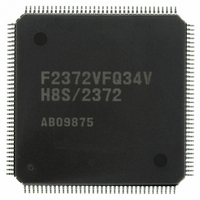
Manufacturer Part Number
DF2372VFQ34V
Description
IC H8S/2372 MCU FLASH 144LQFP
Manufacturer
Renesas Electronics America
Series
H8® H8S/2300r
Datasheet
1.YR0K42378FC000BA.pdf
(1208 pages)
Specifications of DF2372VFQ34V
Core Processor
H8S/2000
Core Size
16-Bit
Speed
34MHz
Connectivity
I²C, IrDA, SCI, SmartCard
Peripherals
DMA, POR, PWM, WDT
Number Of I /o
96
Program Memory Size
256KB (256K x 8)
Program Memory Type
FLASH
Ram Size
32K x 8
Voltage - Supply (vcc/vdd)
3 V ~ 3.6 V
Data Converters
A/D 16x10b; D/A 6x8b
Oscillator Type
External
Operating Temperature
-20°C ~ 75°C
Package / Case
144-LQFP
For Use With
YLCDRSK2378 - KIT DEV EVAL H8S/2378 LCDYR0K42378FC000BA - KIT EVAL FOR H8S/2378HS0005KCU11H - EMULATOR E10A-USB H8S(X),SH2(A)
Lead Free Status / RoHS Status
Lead free / RoHS Compliant
Eeprom Size
-
Available stocks
Company
Part Number
Manufacturer
Quantity
Price
Company:

Part Number:
DF2372VFQ34V
Manufacturer:
Renesas Electronics America
Quantity:
10 000


Item
21.4.2 User Program
Mode
(2) Programming
Procedure in User
Program Mode
6. The FPEFEQ and
FUBRA parameters are
set for initialization.
21.8 Serial
Communication
Interface Specification
for Boot Mode
(4) Inquiry and
Selection States
(b) Device Selection
Figure 21.21
Programming
Sequence
(9) Programming/
Erasing State
(b) 128-byte
programming
24.2.1 Clock Division
Mode
25.2 Register Bits
Page
889
930
942
943
972
1004
Revision (See Manual for Details)
Description amended
…For details on the frequency setting, see the description in
21.3.2 (2) (a), Flash programming/erasing frequency parameter
(FPEFEQ: general register ER0 of CPU).
…For details, see the descriptions in 21.3.2 (2) (a), Flash
programming/erasing frequency parameter (FPEFEQ: general
register ER0 of CPU), and 21.3.2 (2) (b), Flash user branch
address setting parameter (FUBRA: general register ER1 of
CPU).
Description amended
•
Figure amended
Description amended
• Programming Address (four bytes): Start address for
programming
Multiple of the size specified in response to the programming
unit inquiry (i.e. H'00, H'01, H'00, H'00 : H'00010000)
Description amended
…In clock division mode, the CPU, bus masters, and on-chip
peripheral functions all operate on the operating clock (1/2,
1/4 ) specified by bits SCK2 to SCK0.
Table amended
Register
Abbreviation Bit 7
FCCS *
Host
Size (one byte): Amount of device-code data
This is fixed at 4
8
—
Programming selection (H'42, H'43
Bit 6
—
Bit 5
—
Rev.7.00 Mar. 18, 2009 page xvii of lxvi
Bit 4
FLER
Bit 3
—
)
Bit 2
—
REJ09B0109-0700
Bit 1
—
Boot program
Transfer of the
programming
program
Bit 0
SCO
Module
FLASH
Related parts for DF2372VFQ34V
Image
Part Number
Description
Manufacturer
Datasheet
Request
R

Part Number:
Description:
KIT STARTER FOR M16C/29
Manufacturer:
Renesas Electronics America
Datasheet:

Part Number:
Description:
KIT STARTER FOR R8C/2D
Manufacturer:
Renesas Electronics America
Datasheet:

Part Number:
Description:
R0K33062P STARTER KIT
Manufacturer:
Renesas Electronics America
Datasheet:

Part Number:
Description:
KIT STARTER FOR R8C/23 E8A
Manufacturer:
Renesas Electronics America
Datasheet:

Part Number:
Description:
KIT STARTER FOR R8C/25
Manufacturer:
Renesas Electronics America
Datasheet:

Part Number:
Description:
KIT STARTER H8S2456 SHARPE DSPLY
Manufacturer:
Renesas Electronics America
Datasheet:

Part Number:
Description:
KIT STARTER FOR R8C38C
Manufacturer:
Renesas Electronics America
Datasheet:

Part Number:
Description:
KIT STARTER FOR R8C35C
Manufacturer:
Renesas Electronics America
Datasheet:

Part Number:
Description:
KIT STARTER FOR R8CL3AC+LCD APPS
Manufacturer:
Renesas Electronics America
Datasheet:
Part Number:
Description:
KIT STARTER FOR RX610
Manufacturer:
Renesas Electronics America
Datasheet:

Part Number:
Description:
KIT STARTER FOR R32C/118
Manufacturer:
Renesas Electronics America
Datasheet:

Part Number:
Description:
KIT DEV RSK-R8C/26-29
Manufacturer:
Renesas Electronics America
Datasheet:

Part Number:
Description:
KIT STARTER FOR SH7124
Manufacturer:
Renesas Electronics America
Datasheet:

Part Number:
Description:
KIT STARTER FOR H8SX/1622
Manufacturer:
Renesas Electronics America
Datasheet:

Part Number:
Description:
KIT DEV FOR SH7203
Manufacturer:
Renesas Electronics America
Datasheet: