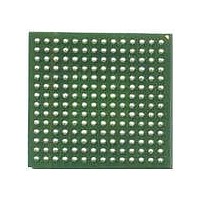
MCF5272VM66J Freescale Semiconductor, MCF5272VM66J Datasheet - Page 337

MCF5272VM66J
Manufacturer Part Number
MCF5272VM66J
Description
IC MCU 166MHZ 196MAPBGA
Manufacturer
Freescale Semiconductor
Series
MCF527xr
Datasheets
1.MCF5272CVF66J.pdf
(544 pages)
2.MCF5272CVF66J.pdf
(12 pages)
3.MCF5272VM66J.pdf
(44 pages)
Specifications of MCF5272VM66J
Core Processor
Coldfire V2
Core Size
32-Bit
Speed
66MHz
Connectivity
EBI/EMI, Ethernet, I²C, SPI, UART/USART, USB
Peripherals
DMA, WDT
Number Of I /o
32
Program Memory Size
16KB (4K x 32)
Program Memory Type
ROM
Ram Size
1K x 32
Voltage - Supply (vcc/vdd)
3 V ~ 3.6 V
Oscillator Type
External
Operating Temperature
0°C ~ 70°C
Package / Case
196-MAPBGA
Processor Series
MCF527x
Core
ColdFire V2
Data Bus Width
32 bit
Data Ram Size
64 KB
Interface Type
I2C, UART, Ethernet, SPI, USB, QSPI
Maximum Clock Frequency
166 MHz
Number Of Timers
4
Operating Supply Voltage
1.4 V to 1.6 V
Maximum Operating Temperature
+ 85 C
Mounting Style
SMD/SMT
3rd Party Development Tools
JLINK-CF-BDM26, EWCF
Development Tools By Supplier
NNDK-MOD5272-KIT, NNDK-MOD5270-KIT
Minimum Operating Temperature
- 40 C
Lead Free Status / RoHS Status
Lead free / RoHS Compliant
Eeprom Size
-
Data Converters
-
Lead Free Status / Rohs Status
Lead free / RoHS Compliant
Available stocks
Company
Part Number
Manufacturer
Quantity
Price
Company:
Part Number:
MCF5272VM66J
Manufacturer:
FREESCAL
Quantity:
416
Company:
Part Number:
MCF5272VM66J
Manufacturer:
Freescale
Quantity:
178
Company:
Part Number:
MCF5272VM66J
Manufacturer:
Freescale Semiconductor
Quantity:
10 000
- Current page: 337 of 544
- Download datasheet (7Mb)
In the above example, CODEC 1 transmits and receives in the B3 time slot once the U transceiver has
completed the D channel. From the rising edge of FSC1, this is at least 19 DCL clocks later. In
Figure
channel. For example, let us say this is 1 DCL clocks long. This defines the programmable delay 1 value
to be 20, (19 + 1), or 0x0014. The DFSC3 signal synchronizes CODECs 3 and 4, and the rising edge of
this frame sync occurs 20 clocks after DFSC2, therefore 40 DCL clocks after FSC1. This defines the value
for programmable delay 3 to be 40, (19 + 1 + 20), or 0x0028.
13.6.5
In this example, ports 0 and 1 are connected to two S/T transceivers. Ports 0 and 1 are programmed in
slave mode. Ports 2 and 3 are not used, and may be disabled.
Freescale Semiconductor
DFSC2
DFSC3
Dout1
FSC1
Din1/
DCL
13-40, a short, optional delay, is shown between the end of the D channel and the start of the B3
Example 3: Two-Line Remote Access with Ports 0 and 1
B1
U Transceiver
MCF5272 ColdFire
MCF5272
D
Interface 1
Interface 0
B2
Figure 13-40. Standard IDL2 10-Bit Mode
Figure 13-41. Two-Line Remote Access
DREQ1
DREQ0
DGNT1
DGNT0
®
Dout1
Dout0
FSC1
DCL1
FSC0
DCL0
D
Din1
Integrated Microprocessor User’s Manual, Rev. 3
Din0
CODEC 1
B3
CODEC 2
B4
Tx
IDL SYNC
Tx
Rx
IDL SYNC
Rx
DGrant
IDL CLK
DGrant
DRequest
IDL CLK
DRequest
MC145574 #1
MC145574 #2
Physical Layer Interface Controller (PLIC)
CODEC 3
B5
CODEC 4
B6
13-41
Related parts for MCF5272VM66J
Image
Part Number
Description
Manufacturer
Datasheet
Request
R
Part Number:
Description:
Mcf5272 Coldfire Integrated Microprocessor User
Manufacturer:
Freescale Semiconductor, Inc
Datasheet:

Part Number:
Description:
MCF5272 Interrupt Service Routine for the Physical Layer Interface Controller
Manufacturer:
Freescale Semiconductor / Motorola
Datasheet:
Part Number:
Description:
Manufacturer:
Freescale Semiconductor, Inc
Datasheet:
Part Number:
Description:
Manufacturer:
Freescale Semiconductor, Inc
Datasheet:
Part Number:
Description:
Manufacturer:
Freescale Semiconductor, Inc
Datasheet:
Part Number:
Description:
Manufacturer:
Freescale Semiconductor, Inc
Datasheet:
Part Number:
Description:
Manufacturer:
Freescale Semiconductor, Inc
Datasheet:
Part Number:
Description:
Manufacturer:
Freescale Semiconductor, Inc
Datasheet:
Part Number:
Description:
Manufacturer:
Freescale Semiconductor, Inc
Datasheet:
Part Number:
Description:
Manufacturer:
Freescale Semiconductor, Inc
Datasheet:
Part Number:
Description:
Manufacturer:
Freescale Semiconductor, Inc
Datasheet:
Part Number:
Description:
Manufacturer:
Freescale Semiconductor, Inc
Datasheet:
Part Number:
Description:
Manufacturer:
Freescale Semiconductor, Inc
Datasheet:
Part Number:
Description:
Manufacturer:
Freescale Semiconductor, Inc
Datasheet:
Part Number:
Description:
Manufacturer:
Freescale Semiconductor, Inc
Datasheet:


