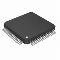
MAXQ622G-0000+ Maxim Integrated Products, MAXQ622G-0000+ Datasheet - Page 9

MAXQ622G-0000+
Manufacturer Part Number
MAXQ622G-0000+
Description
IC MCU 16BIT 64K IR MOD 64LQFP
Manufacturer
Maxim Integrated Products
Series
MAXQ™r
Datasheet
1.MAXQ622G-0000.pdf
(31 pages)
Specifications of MAXQ622G-0000+
Core Processor
RISC
Core Size
16-Bit
Speed
12MHz
Connectivity
I²C, SPI, UART/USART, USB
Peripherals
Brown-out Detect/Reset, Infrared, Power-Fail, POR, WDT
Number Of I /o
44
Program Memory Size
128KB (128K x 8)
Program Memory Type
FLASH
Ram Size
6K x 8
Voltage - Supply (vcc/vdd)
1.7 V ~ 3.6 V
Oscillator Type
Internal
Operating Temperature
0°C ~ 70°C
Package / Case
64-LQFP
Processor Series
MAXQ622
Core
RISC
Data Bus Width
16 bit
Data Ram Size
6 KB
Interface Type
I2C, SPI, USART
Maximum Clock Frequency
12 MHz
Number Of Programmable I/os
44
Number Of Timers
2
Operating Supply Voltage
1.7 V to 3.6 V
Maximum Operating Temperature
+ 70 C
Mounting Style
SMD/SMT
Development Tools By Supplier
MAXQUSBJTAG-KIT MAXQ622-KIT
Minimum Operating Temperature
0 C
For Use With
MAXQ622-KIT# - EVALUATION KIT FOR MAXQ622
Lead Free Status / RoHS Status
Lead free / RoHS Compliant
Eeprom Size
-
Data Converters
-
Lead Free Status / Rohs Status
Details
I
(Notes 6, 21) (Figure 2)
Note 1: Specifications to 0NC are guaranteed by design and are not production tested.
Note 2: V
Note 3: It is not recommended to write to flash when the supply voltage drops below the power-fail warning levels, as there is
Note 4: The power-fail warning monitor and the power-fail reset monitor are designed to track each other with a minimum delta
Note 5: The power-fail reset and POR detectors are designed to operate in tandem to ensure that one or both of these signals
Note 6: Guaranteed by design and not production tested.
Note 7: I
Note 8: The power-check interval (PCI) can be set to always on, or to 1024, 2048, or 4096 nanopower ring clock cycles.
Note 9: Measured on the V
Note 10: Current consumption during POR when powering up while V
Note 11: The minimum amount of time that V
Note 12: The maximum total current, I
Note 13: External clock frequency must be 12MHz to support USB functionality. Full-speed USB(12Mbps)-required bit-rate accu-
Note 14: Programming time does not include overhead associated with utility ROM interface.
2
I
System Frequency
I
Hold Time After (Repeated) START
Clock Low Period
Clock High Period
Setup Time for Repeated START
Hold Time for Data (Notes 22, 23)
Setup Time for Data (Note 24)
SDA/SCL Fall Time (Note 20)
SDA/SCL Rise Time (Note 20)
Setup Time for STOP
Bus Free Time Between STOP and
START
Capacitive Load for Each Bus Line
Noise Margin at the Low Level for
Each Connected Device (Including
Hysteresis)
Noise Margin at the Low Level for
Each Connected Device (Including
Hysteresis)
2
2
C BUS CONTROLLER TIMING
C Bus Operating Frequency
C Bit Rate
listed in the Recommended Operating Conditions table are for the default configuration of 1.8V nominal.
uncertainty in the duration of continuous power supply. The user application should check the status of the power-fail
warning flag before writing to flash to ensure complete write operations.
between the two of 0.11V.
is active at all times when V
achieved.
sink any current. The device is executing code from flash memory.
maximum specified voltage drop. This does not include the IRTX output.
racy is Q2500ppm or Q0.25%. This is inclusive of all potential error sources: frequency tolerance, temperature, aging,
crystal capacitive loading, board layout, etc.
S1
PFW
is measured with the USB data RAM powered down.
PARAMETER
can be programmed to the following nominal voltage trip points: 1.8V, 1.9V, 2.55V, and 2.75V Q3%. The values
_______________________________________________________________________________________
DD
pin and the device not in reset. All inputs are connected to GND or V
Infrared Module and Optional USB
DD
OH(MAX)
< V
t
SYMBOL
t
HIGH_I2C
RST
LOW_I2C
t
V
t
t
t
t
V
DD
HD:DAT
HD:STA
SU:STA
SU:DAT
SU:STO
t
t
nH_I2C
R_I2C
nL_I2C
F_I2C
t
f
f
f
BUF
SYS
C
I2C
I2C
and I
, ensuring the device maintains the reset state until minimum operating voltage is
must be below V
B
OL(MAX)
16-Bit Microcontrollers with
0.1 x V
0.2 x V
, for all listed outputs combined should not exceed 25mA to satisfy the
0.90
MIN
250
STANDARD MODE
4.0
4.7
4.0
4.7
4.0
4.7
0
0
PFW
DD
DD
DD
before a power-fail event is detected.
is less than the POR release voltage.
f
MAX
1000
SYS
3.45
100
300
400
/8
20 + 0.1C
20 + 0.1C
0.1 x V
0.2 x V
MIN
3.60
100
0.6
1.3
0.6
0.6
0.6
1.3
0
0
FAST MODE
DD
DD
DD
B
B
. Outputs do not source/
f
MAX
SYS
400
300
300
400
0.9
/8
UNITS
MHz
kHz
Hz
pF
Fs
Fs
Fs
Fs
Fs
ns
ns
ns
Fs
Fs
V
V
9


