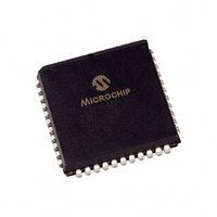
PIC18LF448-I/L Microchip Technology, PIC18LF448-I/L Datasheet - Page 249

PIC18LF448-I/L
Manufacturer Part Number
PIC18LF448-I/L
Description
IC PIC MCU FLASH 8KX16 44PLCC
Manufacturer
Microchip Technology
Series
PIC® 18Fr
Specifications of PIC18LF448-I/L
Core Size
8-Bit
Program Memory Size
16KB (8K x 16)
Core Processor
PIC
Speed
40MHz
Connectivity
CAN, I²C, SPI, UART/USART
Peripherals
Brown-out Detect/Reset, LVD, POR, PWM, WDT
Number Of I /o
33
Program Memory Type
FLASH
Eeprom Size
256 x 8
Ram Size
768 x 8
Voltage - Supply (vcc/vdd)
2 V ~ 5.5 V
Data Converters
A/D 8x10b
Oscillator Type
External
Operating Temperature
-40°C ~ 85°C
Package / Case
44-PLCC
Controller Family/series
PIC18
No. Of I/o's
33
Eeprom Memory Size
256Byte
Ram Memory Size
768Byte
Cpu Speed
40MHz
No. Of Timers
4
Processor Series
PIC18LF
Core
PIC
Data Bus Width
8 bit
Data Ram Size
768 B
Interface Type
SPI, I2C, USART
Maximum Clock Frequency
40 MHz
Number Of Programmable I/os
33
Number Of Timers
4 bit
Operating Supply Voltage
2 V to 5.5 V
Maximum Operating Temperature
+ 85 C
Mounting Style
SMD/SMT
3rd Party Development Tools
52715-96, 52716-328, 52717-734, 52712-325, EWPIC18
Development Tools By Supplier
PG164130, DV164035, DV244005, DV164005, PG164120, ICE2000, DV164136, DM163011
Minimum Operating Temperature
- 40 C
On-chip Adc
8
Lead Free Status / RoHS Status
Lead free / RoHS Compliant
Lead Free Status / RoHS Status
Lead free / RoHS Compliant, Lead free / RoHS Compliant
Available stocks
Company
Part Number
Manufacturer
Quantity
Price
Company:
Part Number:
PIC18LF448-I/L
Manufacturer:
Microchip Technology
Quantity:
10 000
- Current page: 249 of 402
- Download datasheet (7Mb)
20.4
Figure 20-4 shows the operation of the A/D converter
after the GO bit has been set. Clearing the GO/DONE
bit during a conversion will abort the current conver-
sion. The A/D Result register pair will not be updated
with the partially completed A/D conversion sample.
That is, the ADRESH:ADRESL registers will continue
to contain the value of the last completed conversion
(or the last value written to the ADRESH:ADRESL
registers). After the A/D conversion is aborted, a 2 T
wait is required before the next acquisition is started.
After this 2 T
channel is automatically started.
FIGURE 20-3:
© 2006 Microchip Technology Inc.
Note:
A/D Conversions
The GO/DONE bit should NOT be set in
the same instruction that turns on the A/D.
AD
7
0000 00
wait, acquisition on the selected
ADRESH
A/D RESULT JUSTIFICATION
Right Justified
2 1 0 7
ADFM = 1
10-bit Result
ADRESL
0
AD
10-bit Result
20.4.1
The ADRESH:ADRESL register pair is the location
where the 10-bit A/D result is loaded at the completion
of the A/D conversion. This register pair is 16 bits wide.
The A/D module gives the flexibility to left or right justify
the 10-bit result in the 16-bit result register. The A/D
Format Select bit (ADFM) controls this justification.
Figure 20-3 shows the operation of the A/D result justi-
fication. The extra bits are loaded with ‘0’s. When an
A/D result will not overwrite these locations (A/D
disable), these registers may be used as two general
purpose 8-bit registers.
7
ADRESH
10-bit Result
A/D RESULT REGISTERS
ADFM = 0
Left Justified
0 7 6 5
PIC18FXX8
ADRESL
0000 00
DS41159E-page 247
0
Related parts for PIC18LF448-I/L
Image
Part Number
Description
Manufacturer
Datasheet
Request
R

Part Number:
Description:
Manufacturer:
Microchip Technology Inc.
Datasheet:

Part Number:
Description:
Manufacturer:
Microchip Technology Inc.
Datasheet:

Part Number:
Description:
Manufacturer:
Microchip Technology Inc.
Datasheet:

Part Number:
Description:
Manufacturer:
Microchip Technology Inc.
Datasheet:

Part Number:
Description:
Manufacturer:
Microchip Technology Inc.
Datasheet:

Part Number:
Description:
Manufacturer:
Microchip Technology Inc.
Datasheet:

Part Number:
Description:
Manufacturer:
Microchip Technology Inc.
Datasheet:

Part Number:
Description:
Manufacturer:
Microchip Technology Inc.
Datasheet:


