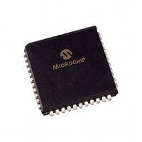
PIC18LF448-I/L Microchip Technology, PIC18LF448-I/L Datasheet - Page 292

PIC18LF448-I/L
Manufacturer Part Number
PIC18LF448-I/L
Description
IC PIC MCU FLASH 8KX16 44PLCC
Manufacturer
Microchip Technology
Series
PIC® 18Fr
Specifications of PIC18LF448-I/L
Core Size
8-Bit
Program Memory Size
16KB (8K x 16)
Core Processor
PIC
Speed
40MHz
Connectivity
CAN, I²C, SPI, UART/USART
Peripherals
Brown-out Detect/Reset, LVD, POR, PWM, WDT
Number Of I /o
33
Program Memory Type
FLASH
Eeprom Size
256 x 8
Ram Size
768 x 8
Voltage - Supply (vcc/vdd)
2 V ~ 5.5 V
Data Converters
A/D 8x10b
Oscillator Type
External
Operating Temperature
-40°C ~ 85°C
Package / Case
44-PLCC
Controller Family/series
PIC18
No. Of I/o's
33
Eeprom Memory Size
256Byte
Ram Memory Size
768Byte
Cpu Speed
40MHz
No. Of Timers
4
Processor Series
PIC18LF
Core
PIC
Data Bus Width
8 bit
Data Ram Size
768 B
Interface Type
SPI, I2C, USART
Maximum Clock Frequency
40 MHz
Number Of Programmable I/os
33
Number Of Timers
4 bit
Operating Supply Voltage
2 V to 5.5 V
Maximum Operating Temperature
+ 85 C
Mounting Style
SMD/SMT
3rd Party Development Tools
52715-96, 52716-328, 52717-734, 52712-325, EWPIC18
Development Tools By Supplier
PG164130, DV164035, DV244005, DV164005, PG164120, ICE2000, DV164136, DM163011
Minimum Operating Temperature
- 40 C
On-chip Adc
8
Lead Free Status / RoHS Status
Lead free / RoHS Compliant
Lead Free Status / RoHS Status
Lead free / RoHS Compliant, Lead free / RoHS Compliant
Available stocks
Company
Part Number
Manufacturer
Quantity
Price
Company:
Part Number:
PIC18LF448-I/L
Manufacturer:
Microchip Technology
Quantity:
10 000
- Current page: 292 of 402
- Download datasheet (7Mb)
BCF
Syntax:
Operands:
Operation:
Status Affected:
Encoding:
Description:
Words:
Cycles:
Example:
DS41159E-page 290
PIC18FXX8
Q Cycle Activity:
Before Instruction
After Instruction
Decode
FLAG_REG = 0xC7
FLAG_REG = 0x47
Q1
register ‘f’
Bit Clear f
[ label ] BCF
0
0
a
0
None
Bit ‘b’ in register ‘f’ is cleared. If ‘a’ is ‘0’,
the Access Bank will be selected, over-
riding the BSR value. If ‘a’ = 1, then the
bank will be selected as per the BSR
value (default).
1
1
BCF
Read
1001
Q2
f
b
[0,1]
f<b>
255
7
FLAG_REG, 7
bbba
Process
f,b[,a]
Data
Q3
ffff
register ‘f’
Write
Q4
ffff
BN
Syntax:
Operands:
Operation:
Status Affected:
Encoding:
Description:
Words:
Cycles:
Example:
Q Cycle Activity:
If Jump:
If No Jump:
Before Instruction
After Instruction
operation
Decode
Decode
No
PC
If Negative
If Negative
Q1
Q1
PC
PC
Read literal
Read literal
operation
Branch if Negative
[ label ] BN
-128
if Negative bit is ‘1’
(PC) + 2 + 2n
None
If the Negative bit is ‘1’, then the
program will branch.
The 2’s complement number ‘2n’ is
added to the PC. Since the PC will have
incremented to fetch the next instruc-
tion, the new address will be
PC + 2 + 2n. This instruction is then a
two-cycle instruction.
1
1(2)
HERE
1110
No
‘n’
‘n’
Q2
Q2
=
=
=
=
=
© 2006 Microchip Technology Inc.
n
address (HERE)
1;
address (Jump)
0;
address (HERE + 2)
127
0110
operation
n
Process
Process
BN
Data
Data
PC
No
Q3
Q3
Jump
nnnn
Write to PC
operation
operation
No
No
Q4
Q4
nnnn
Related parts for PIC18LF448-I/L
Image
Part Number
Description
Manufacturer
Datasheet
Request
R

Part Number:
Description:
Manufacturer:
Microchip Technology Inc.
Datasheet:

Part Number:
Description:
Manufacturer:
Microchip Technology Inc.
Datasheet:

Part Number:
Description:
Manufacturer:
Microchip Technology Inc.
Datasheet:

Part Number:
Description:
Manufacturer:
Microchip Technology Inc.
Datasheet:

Part Number:
Description:
Manufacturer:
Microchip Technology Inc.
Datasheet:

Part Number:
Description:
Manufacturer:
Microchip Technology Inc.
Datasheet:

Part Number:
Description:
Manufacturer:
Microchip Technology Inc.
Datasheet:

Part Number:
Description:
Manufacturer:
Microchip Technology Inc.
Datasheet:


