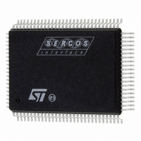
ST92F250CV2QB STMicroelectronics, ST92F250CV2QB Datasheet - Page 252

ST92F250CV2QB
Manufacturer Part Number
ST92F250CV2QB
Description
IC MCU 256K FLASH 100-PQFP
Manufacturer
STMicroelectronics
Series
ST9r
Datasheet
1.ST92F150CV1TB.pdf
(429 pages)
Specifications of ST92F250CV2QB
Core Processor
ST9
Core Size
8/16-Bit
Speed
24MHz
Connectivity
CAN, I²C, LIN, SCI, SPI
Peripherals
DMA, LVD, POR, PWM, WDT
Number Of I /o
80
Program Memory Size
256KB (256K x 8)
Program Memory Type
FLASH
Eeprom Size
1K x 8
Ram Size
8K x 8
Voltage - Supply (vcc/vdd)
4.5 V ~ 5.5 V
Data Converters
A/D 16x10b
Oscillator Type
Internal
Operating Temperature
-40°C ~ 105°C
Package / Case
100-QFP
Processor Series
ST92F25x
Core
ST9
Data Bus Width
8 bit, 16 bit
Data Ram Size
8 KB
Interface Type
CAN, I2C, SCI, SPI
Maximum Clock Frequency
24 MHz
Number Of Programmable I/os
80
Number Of Timers
5 x 16 bit
Operating Supply Voltage
4.5 V to 5.5 V
Maximum Operating Temperature
+ 105 C
Mounting Style
SMD/SMT
Development Tools By Supplier
ST92F150-EPB
Minimum Operating Temperature
- 40 C
On-chip Adc
16 bit x 10 bit
Case
QFP
Lead Free Status / RoHS Status
Lead free / RoHS Compliant
Other names
497-2139
Available stocks
Company
Part Number
Manufacturer
Quantity
Price
Company:
Part Number:
ST92F250CV2QB
Manufacturer:
HKE
Quantity:
30 000
- Current page: 252 of 429
- Download datasheet (8Mb)
SERIAL PERIPHERAL INTERFACE (SPI)
SERIAL PERIPHERAL INTERFACE (Cont’d)
10.7.4 Functional Description
Figure 121
(SPI) block diagram.
This interface contains 4 dedicated registers:
Refer to the SPCR, SPPR, SPSR and SPDR reg-
isters in
10.7.4.1 Master Configuration
In a master configuration, the serial clock is gener-
ated on the SCK pin.
Procedure
252/429
9
– A Control Register (SPCR)
– A Prescaler Register (SPPR)
– A Status Register (SPSR)
– A Data Register (SPDR)
– Define the serial clock baud rate by setting/re-
– Select the CPOL and CPHA bits to define one
– The SS pin must be connected to a high level
– The MSTR and SPOE bits must be set (they
setting the DIV2 bit of SPPR register, by writ-
ing a prescaler value in the SPPR register and
programming the SPR0 & SPR1 bits in the
SPCR register.
of the four relationships between the data
transfer and the serial clock (see
signal during the complete byte transmit se-
quence.
remain set only if the SS pin is connected to a
high level signal).
Section
shows the serial peripheral interface
10.7.6for the bit definitions.
Figure
123).
In this configuration the MOSI pin is a data output
and the MISO pin is a data input.
Transmit Sequence
The transmit sequence begins when a byte is writ-
ten the SPDR register.
The data byte is parallel loaded into the 8-bit shift
register (from the internal bus) during a write cycle
and then shifted out serially to the MOSI pin most
significant bit first.
When data transfer is complete:
During the last clock cycle the SPIF bit is set, a
copy of the data byte received in the shift register
is moved to a buffer. When the SPDR register is
read, the SPI peripheral returns this buffered val-
ue.
Clearing the SPIF bit is performed by the following
software sequence:
1. An access to the SPSR register while the SPIF
2. A read of the SPDR register.
Note: While the SPIF bit is set, all writes to the
SPDR register are inhibited until the SPSR regis-
ter is read.
– The SPIF bit is set by hardware
– An interrupt is generated if the SPIS and SPIE
bit is set
bits are set.
Related parts for ST92F250CV2QB
Image
Part Number
Description
Manufacturer
Datasheet
Request
R

Part Number:
Description:
STMicroelectronics [RIPPLE-CARRY BINARY COUNTER/DIVIDERS]
Manufacturer:
STMicroelectronics
Datasheet:

Part Number:
Description:
STMicroelectronics [LIQUID-CRYSTAL DISPLAY DRIVERS]
Manufacturer:
STMicroelectronics
Datasheet:

Part Number:
Description:
BOARD EVAL FOR MEMS SENSORS
Manufacturer:
STMicroelectronics
Datasheet:

Part Number:
Description:
NPN TRANSISTOR POWER MODULE
Manufacturer:
STMicroelectronics
Datasheet:

Part Number:
Description:
TURBOSWITCH ULTRA-FAST HIGH VOLTAGE DIODE
Manufacturer:
STMicroelectronics
Datasheet:

Part Number:
Description:
Manufacturer:
STMicroelectronics
Datasheet:

Part Number:
Description:
DIODE / SCR MODULE
Manufacturer:
STMicroelectronics
Datasheet:

Part Number:
Description:
DIODE / SCR MODULE
Manufacturer:
STMicroelectronics
Datasheet:

Part Number:
Description:
Search -----> STE16N100
Manufacturer:
STMicroelectronics
Datasheet:

Part Number:
Description:
Search ---> STE53NA50
Manufacturer:
STMicroelectronics
Datasheet:

Part Number:
Description:
NPN Transistor Power Module
Manufacturer:
STMicroelectronics
Datasheet:

Part Number:
Description:
DIODE / SCR MODULE
Manufacturer:
STMicroelectronics
Datasheet:


