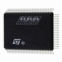
ST92F250CV2QB STMicroelectronics, ST92F250CV2QB Datasheet - Page 393

ST92F250CV2QB
Manufacturer Part Number
ST92F250CV2QB
Description
IC MCU 256K FLASH 100-PQFP
Manufacturer
STMicroelectronics
Series
ST9r
Datasheet
1.ST92F150CV1TB.pdf
(429 pages)
Specifications of ST92F250CV2QB
Core Processor
ST9
Core Size
8/16-Bit
Speed
24MHz
Connectivity
CAN, I²C, LIN, SCI, SPI
Peripherals
DMA, LVD, POR, PWM, WDT
Number Of I /o
80
Program Memory Size
256KB (256K x 8)
Program Memory Type
FLASH
Eeprom Size
1K x 8
Ram Size
8K x 8
Voltage - Supply (vcc/vdd)
4.5 V ~ 5.5 V
Data Converters
A/D 16x10b
Oscillator Type
Internal
Operating Temperature
-40°C ~ 105°C
Package / Case
100-QFP
Processor Series
ST92F25x
Core
ST9
Data Bus Width
8 bit, 16 bit
Data Ram Size
8 KB
Interface Type
CAN, I2C, SCI, SPI
Maximum Clock Frequency
24 MHz
Number Of Programmable I/os
80
Number Of Timers
5 x 16 bit
Operating Supply Voltage
4.5 V to 5.5 V
Maximum Operating Temperature
+ 105 C
Mounting Style
SMD/SMT
Development Tools By Supplier
ST92F150-EPB
Minimum Operating Temperature
- 40 C
On-chip Adc
16 bit x 10 bit
Case
QFP
Lead Free Status / RoHS Status
Lead free / RoHS Compliant
Other names
497-2139
Available stocks
Company
Part Number
Manufacturer
Quantity
Price
Company:
Part Number:
ST92F250CV2QB
Manufacturer:
HKE
Quantity:
30 000
- Current page: 393 of 429
- Download datasheet (8Mb)
MULTIFUNCTION TIMER EXTERNAL TIMING TABLE
(V
Note: The value in the left hand column shows the formula used to calculate the timing minimum or maximum from the oscillator clock period,
standard timer prescaler and counter programmed values.
The value in the right hand two columns show the timing minimum and maximum for an internal clock (INTCLK) at 24MHz.
(1) n = 1 if the input is rising OR falling edge sensitive
(2) In Autodiscrimination mode
Legend:
Tck = INTCLK period = Crystal Oscillator Clock period when CLOCK1 is not divided by 2;
MULTIFUNCTION TIMER EXTERNAL TIMING
N°
1
2
3
4
5
6
7
8
DD
n = 3 if the input is rising AND falling edge sensitive
Symbol
= 5V ± 10%, T
Tw
Tw
Tw
Tw
Tw
Tw
Tw
Tw
OWD
CTW
CTD
AED
LBA
LAB
GW
AD
External clock/trigger pulse width
External clock/trigger pulse distance
Distance between two active edges
Gate pulse width
Distance between TINB pulse edge and the fol-
lowing TINA pulse edge
Distance between TINA pulse edge and the fol-
lowing TINB pulse edge
Distance between two TxINA pulses
Minimum output pulse width/distance
2 x Crystal Oscillator Clock period when CLOCK1 is divided by 2;
Crystal Oscillator Clock period x PLL factor when the PLL is enabled.
A
=
–
40°C to +125°C, C
Parameter
ST92F124/F150/F250 - ELECTRICAL CHARACTERISTICS
Load
= 50pF, f
INTCLK
Formula
n x Tck
n x Tck
3 x Tck
6 x Tck
3 x Tck
= 24MHz, unless otherwise specified)
Tck
Value
n x 42
n x 42
Min
125
250
125
42
0
0
Max
-
-
-
-
-
-
-
-
Unit
ns
ns
ns
ns
ns
ns
ns
ns
393/429
Note
(1)
(1)
(2)
(2)
(2)
1
Related parts for ST92F250CV2QB
Image
Part Number
Description
Manufacturer
Datasheet
Request
R

Part Number:
Description:
STMicroelectronics [RIPPLE-CARRY BINARY COUNTER/DIVIDERS]
Manufacturer:
STMicroelectronics
Datasheet:

Part Number:
Description:
STMicroelectronics [LIQUID-CRYSTAL DISPLAY DRIVERS]
Manufacturer:
STMicroelectronics
Datasheet:

Part Number:
Description:
BOARD EVAL FOR MEMS SENSORS
Manufacturer:
STMicroelectronics
Datasheet:

Part Number:
Description:
NPN TRANSISTOR POWER MODULE
Manufacturer:
STMicroelectronics
Datasheet:

Part Number:
Description:
TURBOSWITCH ULTRA-FAST HIGH VOLTAGE DIODE
Manufacturer:
STMicroelectronics
Datasheet:

Part Number:
Description:
Manufacturer:
STMicroelectronics
Datasheet:

Part Number:
Description:
DIODE / SCR MODULE
Manufacturer:
STMicroelectronics
Datasheet:

Part Number:
Description:
DIODE / SCR MODULE
Manufacturer:
STMicroelectronics
Datasheet:

Part Number:
Description:
Search -----> STE16N100
Manufacturer:
STMicroelectronics
Datasheet:

Part Number:
Description:
Search ---> STE53NA50
Manufacturer:
STMicroelectronics
Datasheet:

Part Number:
Description:
NPN Transistor Power Module
Manufacturer:
STMicroelectronics
Datasheet:

Part Number:
Description:
DIODE / SCR MODULE
Manufacturer:
STMicroelectronics
Datasheet:


