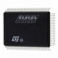
ST92F250CV2QB STMicroelectronics, ST92F250CV2QB Datasheet - Page 44

ST92F250CV2QB
Manufacturer Part Number
ST92F250CV2QB
Description
IC MCU 256K FLASH 100-PQFP
Manufacturer
STMicroelectronics
Series
ST9r
Datasheet
1.ST92F150CV1TB.pdf
(429 pages)
Specifications of ST92F250CV2QB
Core Processor
ST9
Core Size
8/16-Bit
Speed
24MHz
Connectivity
CAN, I²C, LIN, SCI, SPI
Peripherals
DMA, LVD, POR, PWM, WDT
Number Of I /o
80
Program Memory Size
256KB (256K x 8)
Program Memory Type
FLASH
Eeprom Size
1K x 8
Ram Size
8K x 8
Voltage - Supply (vcc/vdd)
4.5 V ~ 5.5 V
Data Converters
A/D 16x10b
Oscillator Type
Internal
Operating Temperature
-40°C ~ 105°C
Package / Case
100-QFP
Processor Series
ST92F25x
Core
ST9
Data Bus Width
8 bit, 16 bit
Data Ram Size
8 KB
Interface Type
CAN, I2C, SCI, SPI
Maximum Clock Frequency
24 MHz
Number Of Programmable I/os
80
Number Of Timers
5 x 16 bit
Operating Supply Voltage
4.5 V to 5.5 V
Maximum Operating Temperature
+ 105 C
Mounting Style
SMD/SMT
Development Tools By Supplier
ST92F150-EPB
Minimum Operating Temperature
- 40 C
On-chip Adc
16 bit x 10 bit
Case
QFP
Lead Free Status / RoHS Status
Lead free / RoHS Compliant
Other names
497-2139
Available stocks
Company
Part Number
Manufacturer
Quantity
Price
Company:
Part Number:
ST92F250CV2QB
Manufacturer:
HKE
Quantity:
30 000
- Current page: 44 of 429
- Download datasheet (8Mb)
ST92F124/F150/F250 - DEVICE ARCHITECTURE
2.6 ADDRESS SPACE EXTENSION
To manage 4 Mbytes of addressing space, it is
necessary to have 22 address bits. The MMU
adds 6 bits to the usual 16-bit address, thus trans-
lating a 16-bit virtual address into a 22-bit physical
address. There are 2 different ways to do this de-
pending on the memory involved and on the oper-
ation being performed.
2.6.1 Addressing 16-Kbyte Pages
This extension mode is implicitly used to address
Data memory space if no DMA is being performed.
The Data memory space is divided into 4 pages of
16 Kbytes. Each one of the four 8-bit registers
(DPR[3:0], Data Page Registers) selects a differ-
ent 16-Kbyte page. The DPR registers allow ac-
cess to the entire memory space which contains
256 pages of 16 Kbytes.
Data paging is performed by extending the 14 LSB
of the 16-bit address with the contents of a DPR
register. The two MSBs of the 16-bit address are
interpreted as the identification number of the DPR
register to be used. Therefore, the DPR registers
Figure 27. Addressing via DPR[3:0]
44/429
9
DPR0
00
DPR1
01
MMU registers
8 bits
22-bit physical address
DPR2
10
DPR3
11
are involved in the following virtual address rang-
es:
The contents of the selected DPR register specify
one of the 256 possible data memory pages. This
8-bit data page number, in addition to the remain-
ing 14-bit page offset address forms the physical
22-bit address (see
A DPR register cannot be modified via an address-
ing mode that uses the same DPR register. For in-
stance, the instruction “POPW DPR0” is legal only
if the stack is kept either in the register file or in a
memory location above 8000h, where DPR2 and
DPR3 are used. Otherwise, since DPR0 and
DPR1 are modified by the instruction, unpredicta-
ble behaviour could result.
14 LSB
DPR0: from 0000h to 3FFFh;
DPR1: from 4000h to 7FFFh;
DPR2: from 8000h to BFFFh;
DPR3: from C000h to FFFFh.
16-bit virtual address
Figure
27).
Related parts for ST92F250CV2QB
Image
Part Number
Description
Manufacturer
Datasheet
Request
R

Part Number:
Description:
STMicroelectronics [RIPPLE-CARRY BINARY COUNTER/DIVIDERS]
Manufacturer:
STMicroelectronics
Datasheet:

Part Number:
Description:
STMicroelectronics [LIQUID-CRYSTAL DISPLAY DRIVERS]
Manufacturer:
STMicroelectronics
Datasheet:

Part Number:
Description:
BOARD EVAL FOR MEMS SENSORS
Manufacturer:
STMicroelectronics
Datasheet:

Part Number:
Description:
NPN TRANSISTOR POWER MODULE
Manufacturer:
STMicroelectronics
Datasheet:

Part Number:
Description:
TURBOSWITCH ULTRA-FAST HIGH VOLTAGE DIODE
Manufacturer:
STMicroelectronics
Datasheet:

Part Number:
Description:
Manufacturer:
STMicroelectronics
Datasheet:

Part Number:
Description:
DIODE / SCR MODULE
Manufacturer:
STMicroelectronics
Datasheet:

Part Number:
Description:
DIODE / SCR MODULE
Manufacturer:
STMicroelectronics
Datasheet:

Part Number:
Description:
Search -----> STE16N100
Manufacturer:
STMicroelectronics
Datasheet:

Part Number:
Description:
Search ---> STE53NA50
Manufacturer:
STMicroelectronics
Datasheet:

Part Number:
Description:
NPN Transistor Power Module
Manufacturer:
STMicroelectronics
Datasheet:

Part Number:
Description:
DIODE / SCR MODULE
Manufacturer:
STMicroelectronics
Datasheet:


