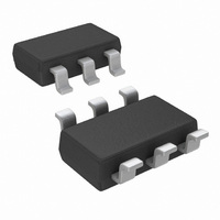
LPV531MK/NOPB National Semiconductor, LPV531MK/NOPB Datasheet

LPV531MK/NOPB
Specifications of LPV531MK/NOPB
LPV531MKTR
Related parts for LPV531MK/NOPB
LPV531MK/NOPB Summary of contents
Page 1
... LPV531 is ideal for use in handheld electronics and portable applications. The LPV531 is manufactured using National’s advanced VIP50 process. A fixed supply current/gain bandwidth is available upon re- quest. Typical Application © 2006 National Semiconductor Corporation Features (Typical 5V supply, unless otherwise noted.) n Supply voltage n Dynamic power mode setting n Continuously programmable supply current — ...
Page 2
... Absolute Maximum Ratings If Military/Aerospace specified devices are required, please contact the National Semiconductor Sales Office/ Distributors for availability and specifications. ESD Tolerance (Note 2) Human Body Model Machine Model V Differential IN + − Supply Voltage ( Storage Temperature Range Junction Temperature (Note 5) 5V Full Power Mode Electrical Characteristics Unless otherwise specified, all limits are guaranteed for T − ...
Page 3
Full Power Mode Electrical Characteristics Unless otherwise specified, all limits are guaranteed for T − 100 kΩ. Boldface limits apply at the temperature extremes. L Symbol Parameter SR Slew Rate (Note 7) GBW Gain Bandwidth ...
Page 4
Mid-Power Mode Electrical Characteristics Unless otherwise specified, all limits are guaranteed for T − V through 100 kΩ resistor 100 kΩ. Boldface limits apply at the temperature extremes. L Symbol Parameter i Input-Referred Current Noise n 5V ...
Page 5
Power Select Electrical Characteristics Unless otherwise specified, all limits are guaranteed for T face limits apply at the temperature extremes. Symbol Parameter t Time from Low Power Mode LF to Full Power Mode t Time from Full Power Mode to ...
Page 6
Typical Performance Characteristics Power Mode the I pin is connected to V SEL for Low Power Mode the I pin is connected to V SEL Supply Current vs. I Supply Current vs. Supply Voltage (Full Power Mode) Supply Current vs. ...
Page 7
Typical Performance Characteristics − Mode the I pin is connected for Mid-Power Mode the I SEL Power Mode the I pin is connected to V SEL Gain and Phase vs. Frequency (Mid Power Mode) Input Offset Voltage ...
Page 8
Typical Performance Characteristics Mode the I pin is connected to V SEL Power Mode the I pin is connected to V SEL PSRR vs. Frequency (Full Power Mode) PSRR vs. Frequency (Low Power Mode) Small Signal Non-Inverting Response (Mid Power ...
Page 9
Typical Performance Characteristics − Mode the I pin is connected for Mid-Power Mode the I SEL Power Mode the I pin is connected to V SEL Large Signal Non-Inverting Response (Full Power Mode) Large Signal Non-Inverting Response ...
Page 10
Typical Performance Characteristics Mode the I pin is connected to V SEL Power Mode the I pin is connected to V SEL Large Signal Inverting Response (Full Power Mode) Large Signal Inverting Response (Low Power Mode) I vs. Supply Current ...
Page 11
Typical Performance Characteristics − Mode the I pin is connected for Mid-Power Mode the I SEL Power Mode the I pin is connected to V SEL Input Referred Voltage Noise vs. Frequency Unless otherwise specified, V pin ...
Page 12
Application Information The LPV531 is an extremely versatile operational amplifier because performance and power consumption can be ad- justed during operation. This provides a method to dynami- cally optimize the supply current, the bandwidth and the output short circuit current ...
Page 13
Application Information 2. Switched Discrete Power Modes In this typical application, the LPV531 can operate at two (or more) power modes in order to fulfill the demands of the design. One of the modes is used to save power. It ...
Page 14
Application Information For the characterized power modes these equations lead to the minimum values in Table 2 below. TABLE 2. Minimum Values for Characterized Power Modes EXT SEL SC 1Ω 9 µ 100 kΩ 0.9 ...
Page 15
Typical Application (Continued) When the load capacitance is increased, the pole at the output will shift to lower frequencies. Eventually, the output pole will shift below the unity gain frequency. This will cause the frequency characteristic to move through the ...
Page 16
Typical Application (Continued) For simplicity, the op amp is modelled as an ideal integrator with a unity gain frequency Hence, its transfer function 0 (or gain) in the frequency domain is A equations in the frequency domain, ...
Page 17
... BANNED SUBSTANCE COMPLIANCE National Semiconductor manufactures products and uses packing materials that meet the provisions of the Customer Products Stewardship Specification (CSP-9-111C2) and the Banned Substances and Materials of Interest Specification (CSP-9-111S2) and contain no ‘‘Banned Substances’’ as defined in CSP-9-111S2. ...


