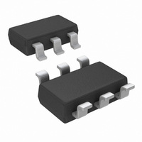
LPV531MK/NOPB National Semiconductor, LPV531MK/NOPB Datasheet - Page 15

LPV531MK/NOPB
Manufacturer Part Number
LPV531MK/NOPB
Description
IC OPAMP PROG R-R OUT TSOT23-6
Manufacturer
National Semiconductor
Series
PowerWise®r
Datasheet
1.LPV531MKNOPB.pdf
(17 pages)
Specifications of LPV531MK/NOPB
Amplifier Type
General Purpose
Number Of Circuits
1
Output Type
Rail-to-Rail
Slew Rate
2.5 V/µs
Gain Bandwidth Product
4.6MHz
Current - Input Bias
0.05pA
Voltage - Input Offset
1000µV
Current - Supply
425µA
Current - Output / Channel
24mA
Voltage - Supply, Single/dual (±)
2.7 V ~ 5.5 V
Operating Temperature
-40°C ~ 85°C
Mounting Type
Surface Mount
Package / Case
TSOT-23-6, TSOT-6
Number Of Channels
1
Voltage Gain Db
128 dB
Common Mode Rejection Ratio (min)
72 dB
Input Offset Voltage
4.5 mV at 5 V
Operating Supply Voltage
5 V
Supply Current
0.53 mA at 5 V
Maximum Operating Temperature
+ 85 C
Minimum Operating Temperature
- 40 C
Lead Free Status / RoHS Status
Lead free / RoHS Compliant
-3db Bandwidth
-
Lead Free Status / Rohs Status
Details
Other names
LPV531MK
LPV531MKTR
LPV531MKTR
Typical Application
When the load capacitance is increased, the pole at the
output will shift to lower frequencies. Eventually, the output
pole will shift below the unity gain frequency. This will cause
the frequency characteristic to move through the 0 dB axis
with a slope of 40 dB/decade and a feedback loop formed
around the LPV531 may oscillate. The LPV531 is internally
compensated in such a manner that it will be stable for load
capacitances up to 100 pF.
When the power setting of the LPV531 is reduced, both the
transconductance of the input stage and the transconduc-
tance of the output stage will scale lineary with the power
level to lower levels. This means that both the unity gain
frequency and the pole to the transconductance of the output
stage and the load capacitance will move down. Because
both the unity gain frequency and the output pole move
down in similar amounts, the stability of the LPV531 is still
the same. This is shown in Figure 7 which gives the phase
margin as a function of the load capacitance in the low power
mode (5 µA), mid-power mode (40 µA) and high power mode
(400 µA). Though the power level and unity gain frequency
move with about two decades, the phase margin as a func-
tion of the capacitive load is hardly affected. This means that
when the LPV531 is stable in an application circuit with a
given load capacitance in the high power mode, the circuit
will remain stable with the same capacitive load connected
when the power level is reduced.
Figure 8 shows a method that is sometimes used to allow an
op amp to drive larger capacitors than it was originally de-
signed to do. The capacitive load is isolated from the output
of the op amp with an isolation resistor (R
the output pole, that was originally located at g
higher frequency. This method requires that the value of
R
LPV531, this method will not be effective when used across
a broad range of power levels. This is because the high
power mode will require a relatively small value for R
while such a small R
levels. In most applications this should not be a problem as
ISO
is in the same order of magnitude as 1/g
FIGURE 7. Phase Margin vs. Capacitive Load
ISO
will be ineffective at low power
(Continued)
ISO
). This moves
m,out
m,out
20132370
. For the
/C
l
, to a
ISO
,
15
the LPV531 can drive sufficient capacitive loads without the
need for an external isolation resistor.
INPUT CAPACITANCE AND FEEDBACK CIRCUIT
ELEMENTS
The LPV531 has a very low input bias current (50 fA). To
obtain this performance a large CMOS input stage is used,
which adds to the input capacitance of the op amp, C
Though this does not affect the DC and low frequency per-
formance, at higher frequencies the input capacitance inter-
acts with the input and the feedback impedances to create a
pole, which results in lower phase margin and gain peaking.
The gain peaking can be reduced by carefully choosing the
appropriate feedback resistor, as well as, by using a feed-
back capacitance, C
shown in Figure 9, if C
loop gain of the op amp is considered infinite then the gain of
the circuit is −R
dominant pole, which causes its gain to drop with frequency.
Hence, this gain is only valid for DC and low frequency. To
understand the effect of the input capacitance coupled with
the non-ideal gain of the op amp, the circuit needs to be
analyzed in the frequency domain using a Laplace trans-
form.
FIGURE 8. Compensation by Isolation Resistor
FIGURE 9. Inverting Amplifier
2
/R
1
F
. An op amp, however, usually has a
. For example, in the inverting amplifier
IN
and C
F
are ignored and the open
20132338
www.national.com
20132325
IN
.


