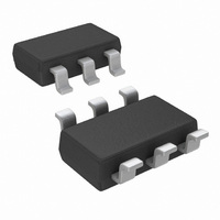
LPV531MK/NOPB National Semiconductor, LPV531MK/NOPB Datasheet - Page 14

LPV531MK/NOPB
Manufacturer Part Number
LPV531MK/NOPB
Description
IC OPAMP PROG R-R OUT TSOT23-6
Manufacturer
National Semiconductor
Series
PowerWise®r
Datasheet
1.LPV531MKNOPB.pdf
(17 pages)
Specifications of LPV531MK/NOPB
Amplifier Type
General Purpose
Number Of Circuits
1
Output Type
Rail-to-Rail
Slew Rate
2.5 V/µs
Gain Bandwidth Product
4.6MHz
Current - Input Bias
0.05pA
Voltage - Input Offset
1000µV
Current - Supply
425µA
Current - Output / Channel
24mA
Voltage - Supply, Single/dual (±)
2.7 V ~ 5.5 V
Operating Temperature
-40°C ~ 85°C
Mounting Type
Surface Mount
Package / Case
TSOT-23-6, TSOT-6
Number Of Channels
1
Voltage Gain Db
128 dB
Common Mode Rejection Ratio (min)
72 dB
Input Offset Voltage
4.5 mV at 5 V
Operating Supply Voltage
5 V
Supply Current
0.53 mA at 5 V
Maximum Operating Temperature
+ 85 C
Minimum Operating Temperature
- 40 C
Lead Free Status / RoHS Status
Lead free / RoHS Compliant
-3db Bandwidth
-
Lead Free Status / Rohs Status
Details
Other names
LPV531MK
LPV531MKTR
LPV531MKTR
www.national.com
Application Information
For the characterized power modes these equations lead to
the minimum values in Table 2 below.
The smallest load resistor that the LPV531 can drive when in
low power mode is 70.8 kΩ, as shown in Table 2. When
driving smaller loads, such as the 10 kΩ load resistor used in
the Electrical Characteristics table specification, the output
swing in the low power mode is limited. If the application
requires a 10 kΩ load then it is not recommended to use the
LPV531 in low power mode.
I
The I
entire internal bias condition. Therefore, the I
sensitive to parasitic signal coupling. In order to protect the
I
PCB layout such that there is as little coupling between the
I
Typical Application
AC COUPLED CIRCUITS
The programmable power mode makes the LPV531 ideal for
AC coupled circuits where the circuit needs to be kept active
to maintain a quiescent charge on the coupling capacitors
with minimal power consumption. Figure 5 shows the sche-
matic of an inverting AC coupled amplifier using the LPV531
with the I
The advantage of the low power active mode for AC coupled
amplifiers is the elimination of the time needed to re-
establish a quiescent operating point when the amplifier is
switched to full power mode.
When an amplifier without a low power active mode is used
in low power applications, there are two ways to minimize
power consumption. The first method turns off the amplifier
by switching off power to the op amp using a transistor
switch. The second method uses an amplifier with a shut-
down pin. Both of these methods have the problem of allow-
ing the coupling capacitors, C
quiescent DC voltage stored on them when in the shutdown
state. When the amplifier is turned on again, the quiescent
DC voltages must reestablish themselves. During this time,
the amplifier’s output is not usable because the output signal
is a mixture of the amplified input signal and the charging
voltage on the coupling capacitors. The settling time can
range from a several milliseconds to several seconds de-
pending on the resistor and capacitor values.
When the LPV531 is placed into the low power mode, the
power consumption is minimal but the amplifier is active to
maintain the quiescent DC voltage on the coupling capaci-
tors. The transition back to the operational high power mode
is fast, within a few hundred nanoseconds. The active low
power mode of the LPV531 separates two critical aspects of
SEL
SEL
SEL
100 kΩ
1 MΩ
R
1Ω
EXT
pin from unwanted distortion, it is important to route the
pin and the output or other signal traces as possible.
SENSITIVITY
SEL
TABLE 2. Minimum Values for Characterized
SEL
pin is a current reference that directly affects the
0.9 µA
99 nA
9 µA
pin controlled by I/O ports of a microcontroller.
I
SEL
Power Modes
300 µA
55 µA
3 mA
I
SC
1
and C
2
(Continued)
to discharge the
SEL
70.8 kΩ
7.8 kΩ
R
770Ω
LOAD
pin is very
14
a low power AC amplifier design. The values of the gain
resistors, bias resistors, and coupling capacitors can be
chosen independently of the turn-on and stabilization time.
PROGRAMMABLE POWER LEVELS AND THE
EFFECTS OF STABILITY COMPENSATION METHODS
USING EXTERNAL COMPONENTS
In some op amp application circuits, external capacitors are
used to improve the stability of the feedback loop around the
amplifier. When using the programmable power level feature
of the LPV531 such stability improvement methods may not
work. This is related to the internal frequency compensation
method applied inside the LPV531.
Figure 6 shows the bode plot of the frequency response of
the LPV531. The gain-bandwidth product is determined by
the transconductance of the input stage (g
ternal Miller compensation capacitor (C
dominant pole is formed by the transconductance of the
output stage (g
the output of the LPV531 (C
crosses the frequency axis with a single-pole slope
(20 dB/decade). This ensures the stability of feedback loops
formed around the LPV531.
FIGURE 6. Bode Plot of the Frequency Response
FIGURE 5. Inverting AC Coupled Application
m,out
) and the load capacitance connected to
l
). The frequency response
m,in
m
). The non-
) and the in-
20132371
20132334


