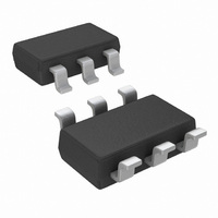
LPV531MK/NOPB National Semiconductor, LPV531MK/NOPB Datasheet - Page 2

LPV531MK/NOPB
Manufacturer Part Number
LPV531MK/NOPB
Description
IC OPAMP PROG R-R OUT TSOT23-6
Manufacturer
National Semiconductor
Series
PowerWise®r
Datasheet
1.LPV531MKNOPB.pdf
(17 pages)
Specifications of LPV531MK/NOPB
Amplifier Type
General Purpose
Number Of Circuits
1
Output Type
Rail-to-Rail
Slew Rate
2.5 V/µs
Gain Bandwidth Product
4.6MHz
Current - Input Bias
0.05pA
Voltage - Input Offset
1000µV
Current - Supply
425µA
Current - Output / Channel
24mA
Voltage - Supply, Single/dual (±)
2.7 V ~ 5.5 V
Operating Temperature
-40°C ~ 85°C
Mounting Type
Surface Mount
Package / Case
TSOT-23-6, TSOT-6
Number Of Channels
1
Voltage Gain Db
128 dB
Common Mode Rejection Ratio (min)
72 dB
Input Offset Voltage
4.5 mV at 5 V
Operating Supply Voltage
5 V
Supply Current
0.53 mA at 5 V
Maximum Operating Temperature
+ 85 C
Minimum Operating Temperature
- 40 C
Lead Free Status / RoHS Status
Lead free / RoHS Compliant
-3db Bandwidth
-
Lead Free Status / Rohs Status
Details
Other names
LPV531MK
LPV531MKTR
LPV531MKTR
www.national.com
V
∆V
TC V
I
CMRR
PSRR
CMVR
A
V
I
I
B
SC
S
Symbol
OS
VOL
O
Absolute Maximum Ratings
If Military/Aerospace specified devices are required,
please contact the National Semiconductor Sales Office/
Distributors for availability and specifications.
5V Full Power Mode Electrical Characteristics
Unless otherwise specified, all limits are guaranteed for T
V
OS
−
ESD Tolerance (Note 2)
V
Supply Voltage (V
Storage Temperature Range
Junction Temperature (Note 5)
, R
IN
OS
Human Body Model
Machine Model
Differential
L
= 100 kΩ. Boldface limits apply at the temperature extremes.
Input Offset Voltage
Input Offset Voltage Difference (V
Input Offset Average Drift
Input Bias Current
Common Mode Rejection
Ratio
Power Supply Rejection Ratio
Input Common Mode Voltage
Range
Large Signal Voltage Gain
Output Swing High
Output Swing Low
Output Short Circuit Current
(Note 3)
Supply Current
+
Parameter
- V
−
)
−65˚C to +150˚C
(V
(Note 8)
(Note 9)
V
V
V
CMRR ≥ 50 dB
V
R
V
R
V
R
R
R
R
R
R
R
Sourcing, V
V
Sinking, V
V
CM
+
CM
O
O
O
ID
ID
L
L
L
L
L
L
L
L
L
OS
OS
= 2.7V to 5.5V
= 1 kΩ to V
= 10 kΩ to V
= 100 kΩ, to V
= 1 kΩ to V
= 10 kΩ to V
= 100 kΩ to V
= 1 kΩ to V
= 10 kΩ to V
= 100 kΩ to V
= 0.5V to 4.5V
= 0.5V to 4.5V
= 0.5V to 4.5V
= 100 mV
= −100 mV
(Note 1)
Stepped from 0V to 3.5V
= 1V
in Full Power Mode) −
in Low Power Mode)
+150˚C
2000V
200V
O
±
O
2V
6V
= 2.5V
Conditions
= 2.5V
J
+
+
+
= 25˚C, V
/2
/2
/2
+
+
+
/2
/2
/2
+
+
+
/2
/2
/2
2
Operating Ratings
Operating Temperature Range
Supply Voltage (V
Package Thermal Resistance (θ
Soldering Information
(10 sec)
+
6-Pin TSOT23
= 5V, V
Infrared or Convection (20 sec)
Wave Soldering Lead Temp.
−
= 0V, V
(Note 6)
−0.3
Min
104
100
108
104
72
68
74
70
87
84
13
10
+
– V
CM
−
= V
)
O
(Note 5)
±
= V
Typ
114
128
120
160
105
−15
425
.05
±
±
95
90
96
55
30
95
24
0.1
(Note 1)
1
2
JA
+
/2, I
) (Note 4)
SEL
(Note 6)
±
±
Max
±
180
195
210
230
120
135
120
135
530
650
pin connected to
3.8
±
±
80
85
50
60
−8
−3
100
4.5
10
5
2
−40˚C to +85˚C
2.7V to 5.5V
235˚C
260˚C
mV from
171˚C/W
Units
µV/˚C
mV
mV
mV
mA
pA
dB
dB
dB
µA
V
V
+


