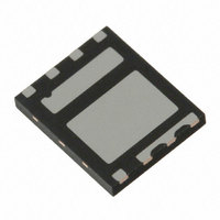
FDMS7602S Fairchild Semiconductor, FDMS7602S Datasheet

FDMS7602S
Specifications of FDMS7602S
Available stocks
Related parts for FDMS7602S
FDMS7602S Summary of contents
Page 1
... Thermal Resistance, Junction to Case θJC Package Marking and Ordering Information Device Marking Device FDMS7602S FDMS7602S ©2010 Fairchild Semiconductor Corporation FDMS7602S Rev.C1 ® MOSFET General Description This device includes two specialized N-Channel MOSFETs in a dual MLP package.The switch node has been internally = ...
Page 2
... Fall Time f Q Total Gate Charge g Q Total Gate Charge g Q Gate to Source Gate Charge gs Q Gate to Drain “Miller” Charge gd ©2010 Fairchild Semiconductor Corporation FDMS7602S Rev. °C unless otherwise noted J Test Conditions = 250 μ mA 250 μA, referenced to 25 °C I ...
Page 3
... Pulse Test: Pulse Width < 300 μs, Duty cycle < 2.0 N-ch device, the negative Vgs rating is for low duty cycle pulse ocurrence only. No continuous rating is implied. ©2010 Fairchild Semiconductor Corporation FDMS7602S Rev. °C unless otherwise noted J Test Conditions ...
Page 4
... PULSE DURATION = 80 s DUTY CYCLE = 0.5% MAX 150 1.5 2.0 2 GATE TO SOURCE VOLTAGE (V) GS Figure 5. Transfer Characteristics ©2010 Fairchild Semiconductor Corporation FDMS7602S Rev. 25°C unless otherwise noted J μ PULSE DURATION = 80 s DUTY CYCLE = 0.5% MAX 1.5 2 100 125 150 - 0.001 3.0 3.5 4.0 ...
Page 5
... Limited by Package CASE TEMPERATURE ( , T C Figure 9. Maximum Continuous Drain Current vs Case Temperature 1000 100 Figure 11. Single Pulse Maximum Power Dissipation ©2010 Fairchild Semiconductor Corporation FDMS7602S Rev. 25°C unless otherwise noted J 2000 1000 100 3.5 C/W θ JC 0.1 0.01 100 125 ...
Page 6
... Typical Characteristics (Q1 N-Channel) 2 DUTY CYCLE-DESCENDING ORDER 0.5 0.2 0.1 0.05 0.1 0.02 0.01 0.01 0.001 - Figure 12. Junction-to-Ambient Transient Thermal Response Curve ©2010 Fairchild Semiconductor Corporation FDMS7602S Rev. 25°C unless otherwise noted J SINGLE PULSE 125 C/W θ Note RECTANGULAR PULSE DURATION (sec) ...
Page 7
... PULSE DURATION = 80 s DUTY CYCLE = 0.5% MAX 125 1.5 2.0 2 GATE TO SOURCE VOLTAGE (V) GS Figure 17. Transfer Characteristics ©2010 Fairchild Semiconductor Corporation FDMS7602S Rev.C1 μ s 1.5 2.0 Figure 14. Normalized on-Resistance vs Drain 50 75 100 125 150 - 0.01 3.0 3.5 5 PULSE DURATION = 80 DUTY CYCLE = 0.5% MAX 4 ...
Page 8
... 4 Limited by package CASE TEMPERATURE ( , T C Figure 21. Maximum Continuous Drain Current vs Case Temperature 1000 100 ©2010 Fairchild Semiconductor Corporation FDMS7602S Rev.C1 3000 1000 100 100 C/W θ 0.1 0.01 100 125 150 Figure 22. Forward Bias Safe Operating Area - PULSE WIDTH (sec) Figure 23 ...
Page 9
... Typical Characteristics (Q2 SyncFET) 2 DUTY CYCLE-DESCENDING ORDER 0.5 0.2 0.1 0.05 0.1 0.02 0.01 0.01 0.001 - Figure 24. Junction-to-Ambient Transient Thermal Response Curve ©2010 Fairchild Semiconductor Corporation FDMS7602S Rev.C1 SINGLE PULSE 120 C/W θ Note RECTANGULAR PULSE DURATION (sec NOTES: DUTY FACTOR PEAK T ...
Page 10
... 100 TIME (ns) Figure FDMS7602S SyncFET body diode reverse recovery characteristic ©2010 Fairchild Semiconductor Corporation FDMS7602S Rev.C1 (continued) Schottky barrier diodes exhibit significant leakage at high tem- perature and high reverse voltage. This will increase the power in the device. 10000 1000 μ ...
Page 11
... Dimensional Outline and Pad Layout ©2010 Fairchild Semiconductor Corporation FDMS7602S Rev.C1 www.fairchildsemi.com ...
Page 12
... Product Status Advance Information Formative / In Design Preliminary First Production No Identification Needed Full Production Obsolete Not In Production ©2010 Fairchild Semiconductor Corporation FDMS7602S Rev.C1 F-PFS™ Power-SPM™ ® FRFET PowerTrench SM Global Power Resource PowerXS™ Green FPS™ Programmable Active Droop™ ...


