SI8465DB-T2-E1 Vishay, SI8465DB-T2-E1 Datasheet
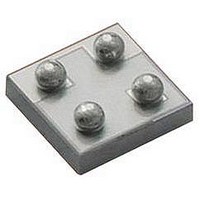
MOSFET P-CH D-S 20V MICROFOOT

SI8465DB-T2-E1

Manufacturer Part Number
SI8465DB-T2-E1
Description
MOSFET P-CH D-S 20V MICROFOOT
Manufacturer
Vishay
Series
TrenchFET®r
Datasheet

Specifications of SI8465DB-T2-E1

Fet Type
MOSFET P-Channel, Metal Oxide
Fet Feature
Logic Level Gate
Rds On (max) @ Id, Vgs
104 mOhm @ 1.5A, 4.5V
Drain To Source Voltage (vdss)
20V
Vgs(th) (max) @ Id
1.5V @ 250µA
Gate Charge (qg) @ Vgs
18nC @ 10V
Input Capacitance (ciss) @ Vds
450pF @ 10V
Power - Max
780mW
Mounting Type
Surface Mount
Package / Case
4-MICRO FOOT®CSP
Transistor Polarity
P Channel
Continuous Drain Current Id
-3.8A
Drain Source Voltage Vds
-20V
On Resistance Rds(on)
104mohm
Rds(on) Test Voltage Vgs
-4.5V
Threshold Voltage Vgs Typ
-1.5V
Resistance Drain-source Rds (on)
0.122 Ohms
Forward Transconductance Gfs (max / Min)
7 S
Drain-source Breakdown Voltage
- 20 V
Continuous Drain Current
- 3.8 A
Power Dissipation
1.8 W
Maximum Operating Temperature
+ 85 C
Mounting Style
SMD/SMT
Minimum Operating Temperature
- 40 C
Lead Free Status / RoHS Status
Lead free / RoHS Compliant
Current - Continuous Drain (id) @ 25° C
-
Lead Free Status / Rohs Status
 Details
Other names
SI8465DB-T2-E1TR
Notes:
a. Surface mounted on 1" x 1" FR4 board with full copper, t = 10 s.
b. Surface mounted on 1" x 1" FR4 board with minimum copper, t = 10 s.
c. Refer to IPC/JEDEC (J-STD-020C), no manual or hand soldering.
d. In this document, any reference to case represents the body of the MICRO FOOT device and foot is the bump.
e. Based on T
Document Number: 65363
S09-1922-Rev. A, 28-Sep-09
Ordering Information: Si8465DB-T2-E1 (Lead (Pb)-free and Halogen-free)
PRODUCT SUMMARY
ABSOLUTE MAXIMUM RATINGS T
Parameter
Drain-Source Voltage
Gate-Source Voltage
Continuous Drain Current (T
Pulsed Drain Current
Continuous Source-Drain Diode Current
Maximum Power Dissipation
Operating Junction and Storage Temperature Range
Package Reflow Conditions
V
DS
- 20
(V)
Device Marking: 8465
Bump Side View
S
S
A
2
3
= 25 °C.
0.104 at V
0.148 at V
R
G
D
MICRO FOOT
DS(on)
xxx = Date/Lot Traceability Code
1
4
GS
GS
c
(Ω)
= - 4.5 V
= - 2.5 V
J
= 150 °C)
Backside View
P-Channel 20-V (D-S) MOSFET
I
D
- 3.8
- 3.2
(A)
a, e
A
= 25 °C, unless otherwise noted
Q
IR/Convection
g
T
T
T
T
T
T
T
T
T
T
6 nC
(Typ.)
A
A
A
A
C
A
A
A
A
A
= 25 °C
= 70 °C
= 25 °C
= 70 °C
= 25 °C
= 25 °C
= 25 °C
= 70 °C
= 25 °C
= 70 °C
VPR
FEATURES
APPLICATIONS
• Halogen-free According to IEC 61249-2-21
• TrenchFET
• Compliant to RoHS Directive 2002/95/EC
• Load Switches, Battery Switches and Charger Switches
• DC/DC Converters
Symbol
T
J
Definition
in Portable Device Applications
V
V
I
P
, T
DM
I
I
GS
DS
D
S
D
stg
®
Power MOSFET
G
P-Channel MOSFET
- 55 to 150
- 0.65
- 3.8
- 2.5
- 2.0
- 1.5
Limit
0.78
± 12
1.8
1.1
0.5
- 20
- 15
260
- 3
260
a
a
a
b
a
b
b
a
b
S
D
b
Vishay Siliconix
Si8465DB
www.vishay.com
Unit
°C
W
V
A
1

Related parts for SI8465DB-T2-E1

SI8465DB-T2-E1 Summary of contents

Page 1

... Backside View Device Marking: 8465 xxx = Date/Lot Traceability Code Ordering Information: Si8465DB-T2-E1 (Lead (Pb)-free and Halogen-free) ABSOLUTE MAXIMUM RATINGS T Parameter Drain-Source Voltage Gate-Source Voltage Continuous Drain Current (T = 150 °C) J Pulsed Drain Current Continuous Source-Drain Diode Current Maximum Power Dissipation Operating Junction and Storage Temperature Range ...

Page 2

... Si8465DB Vishay Siliconix THERMAL RESISTANCE RATINGS Parameter a, b Maximum Junction-to-Ambient c, d Maximum Junction-to-Ambient Notes: a. Surface mounted on 1" x 1" FR4 board with full copper. b. Maximum under steady state conditions is 100 °C/W. c. Surface mounted on 1" x 1" FR4 board with minimum copper. d. Maximum under steady state conditions is 190 °C/W. ...

Page 3

... Total Gate Charge (nC) g Gate Charge Document Number: 65363 S09-1922-Rev. A, 28-Sep- thru 2 1 2.0 2.5 3 Si8465DB Vishay Siliconix 125 ° ° ° 0.0 0.5 1.0 1 Gate-to-Source Voltage (V) GS Transfer Characteristics 800 C iss 600 400 C oss 200 C rss Drain-to-Source Voltage (V) ...

Page 4

... Si8465DB Vishay Siliconix TYPICAL CHARACTERISTICS 25 °C, unless otherwise noted 100 150 ° 0.1 0.0 0.3 0 Source-to-Drain Voltage (V) SD Source-Drain Diode Forward Voltage 1 250 µA D 1.2 1.1 1.0 0.9 0.8 0.7 0 Temperature (°C) J Threshold Voltage www.vishay.com °C J 0.9 1.2 1.5 75 100 125 ...

Page 5

... It is used to determine the current rating, when this rating falls below the package limit. Document Number: 65363 S09-1922-Rev. A, 28-Sep-09 100 125 150 = 150 °C, using junction-to-case thermal resistance, and is more useful in settling the upper J(max) Si8465DB Vishay Siliconix 1.5 1.2 0.9 0.6 0.3 0.0 25 ...

Page 6

... Si8465DB Vishay Siliconix TYPICAL CHARACTERISTICS 25 °C, unless otherwise noted 1 Duty Cycle = 0.5 0.2 0.1 0.1 0.05 0.02 Single Pulse 0. Normalized Thermal Transient Impedance, Junction-to-Ambient (1" x 1" FR4 Board with Full Copper) 1 Duty Cycle = 0.5 0.2 0.1 0.1 0.05 0.02 Single Pulse ...

Page 7

... Millimeters Nom. Max. 0.505 0.548 0.250 0.280 0.255 0.268 0.310 0.320 0.500 0.250 0.270 0.960 1.000 Si8465DB Vishay Siliconix Bump Note Inches Min. Nom. 0.0181 0.0198 0.0086 0.0098 0.0095 0.0100 0.0118 0.0122 0.0197 0.0090 0.0098 0.0362 0.0378 Max. 0.0215 ...

Page 8

... Vishay disclaims any and all liability arising out of the use or application of any product described herein or of any information provided herein to the maximum extent permitted by law. The product specifications do not expand or otherwise modify Vishay’ ...

Related keywords