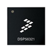
DSP56311VF150R2 Freescale Semiconductor, DSP56311VF150R2 Datasheet - Page 74

DSP56311VF150R2
Manufacturer Part Number
DSP56311VF150R2
Description
IC DSP 24BIT 150MHZ 196-BGA
Manufacturer
Freescale Semiconductor
Series
DSP563xxr
Type
Fixed Pointr
Datasheet
1.DSP56311VL150R2.pdf
(96 pages)
Specifications of DSP56311VF150R2
Interface
Host Interface, SSI, SCI
Clock Rate
150MHz
Non-volatile Memory
ROM (576 B)
On-chip Ram
384kB
Voltage - I/o
3.30V
Voltage - Core
1.80V
Operating Temperature
-40°C ~ 100°C
Mounting Type
Surface Mount
Package / Case
196-MAPBGA
Device Core Size
24b
Format
Fixed Point
Clock Freq (max)
150MHz
Mips
150
Device Input Clock Speed
150MHz
Ram Size
384KB
Operating Supply Voltage (typ)
1.8/3.3V
Operating Supply Voltage (min)
1.7/1.7/3/3/3/3/3/3V
Operating Temp Range
-40C to 100C
Operating Temperature Classification
Industrial
Mounting
Surface Mount
Pin Count
196
Package Type
MA-BGA
Lead Free Status / RoHS Status
Contains lead / RoHS non-compliant
Available stocks
Company
Part Number
Manufacturer
Quantity
Price
Company:
Part Number:
DSP56311VF150R2
Manufacturer:
Freescale Semiconductor
Quantity:
10 000
Design Considerations
The maximum internal current (I
case operation conditions—not necessarily a real application case. The typical internal current (I
reflects the average switching of the internal buses on typical operating conditions. Perform the following steps for
applications that require very low current consumption:
One way to evaluate power consumption is to use a current-per-MIPS measurement methodology to minimize
specific board effects (that is, to compensate for measured board current not caused by the DSP). A benchmark
power consumption test algorithm is listed in Appendix A. Use the test algorithm, specific test current
measurements, and the following equation to derive the current-per-MIPS value.
Note: F1 should be significantly less than F2. For example, F2 could be 66 MHz and F1 could be 33 MHz. The
4.4 PLL Performance Issues
The following explanations should be considered as general observations on expected PLL behavior. There is no
test that replicates these exact numbers. These observations were measured on a limited number of parts and were
not verified over the entire temperature and voltage ranges.
4.4.1
The phase skew of the PLL is defined as the time difference between the falling edges of
given capacitive load on
2, External Clock Timing, on page 2-5 for input frequencies greater than 15 MHz and the MF ≤4, this skew is
greater than or equal to 0.0 ns and less than 1.8 ns; otherwise, this skew is not guaranteed. However, for MF < 10
and input frequencies greater than 10 MHz, this skew is between − 1.4 ns and +3.2 ns.
4-4
Where:
1.
2.
3.
4.
5.
6.
7.
I
I
F2
F1
degree of difference between F1 and F2 determines the amount of precision with which the current rating
can be determined for an application.
typF2
typF1
Equation 4:
Equation 5:
Set the EBD bit when you are not accessing external memory.
Minimize external memory accesses, and use internal memory accesses.
Minimize the number of pins that are switching.
Minimize the capacitive load on the pins.
Connect the unused inputs to pull-up or pull-down resistors.
Disable unused peripherals.
Disable unused pin activity (for example, CLKOUT, XTAL).
Phase Skew Performance
=
=
=
=
⁄
CLKOUT
I
MIPS
=
50
×
=
current at F2
current at F1
high frequency (any specified operating frequency)
low frequency (any specified operating frequency lower than F2)
CCI
, over the entire process, temperature and voltage ranges. As defined in Figure 2-
10
I
⁄
–
max) value reflects the typical possible switching of the internal buses on best-
12
MHz
×
3.3
DSP56311 Technical Data, Rev. 8
=
×
(
I
33
typF2
×
10
–
I
6
typF1
=
5.48 mA
)
⁄
(
F2 F1
–
EXTAL
Freescale Semiconductor
CCItyp
and
CLKOUT
) value
for a


