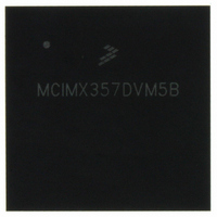
MCIMX357DVM5B Freescale Semiconductor, MCIMX357DVM5B Datasheet - Page 44

MCIMX357DVM5B
Manufacturer Part Number
MCIMX357DVM5B
Description
PROCESSOR MULTIMEDIA 400PBGA
Manufacturer
Freescale Semiconductor
Series
i.MX35r
Datasheet
1.MCIMX35WPDKJ.pdf
(148 pages)
Specifications of MCIMX357DVM5B
Core Processor
ARM11
Core Size
32-Bit
Speed
532MHz
Connectivity
1-Wire, CAN, EBI/EMI, Ethernet, I²C, MMC, SPI, SSI, UART/USART, USB OTG
Peripherals
DMA, I²S, LCD, POR, PWM, WDT
Number Of I /o
96
Program Memory Type
ROMless
Ram Size
128K x 8
Voltage - Supply (vcc/vdd)
1.33 V ~ 1.47 V
Oscillator Type
External
Operating Temperature
-20°C ~ 70°C
Package / Case
400-BGA
Operating Temperature (min)
-20C
Operating Temperature (max)
70C
Operating Temperature Classification
Commercial
Mounting
Surface Mount
Embedded Interface Type
CAN, I2C, SPI, UART, USB
Digital Ic Case Style
BGA
No. Of Pins
400
Operating Temperature Range
-20°C To +70°C
Processor Type
I.MX35
Lead Free Status / RoHS Status
Lead free / RoHS Compliant
Eeprom Size
-
Program Memory Size
-
Data Converters
-
Lead Free Status / Rohs Status
Compliant
Available stocks
Company
Part Number
Manufacturer
Quantity
Price
Company:
Part Number:
MCIMX357DVM5B
Manufacturer:
Freescale Semiconductor
Quantity:
10 000
Part Number:
MCIMX357DVM5B
Manufacturer:
FREESCALE
Quantity:
20 000
Company:
Part Number:
MCIMX357DVM5BR2
Manufacturer:
Freescale Semiconductor
Quantity:
10 000
1
2
3
4
5
6
7
8
9
Note: All configuration parameters (CSA, CSN, WBEA, WBEN, LBA, LBN, OEN, OEA, RBEA, and RBEN) are in cycle units.
44
Ref No.
WE40A
WE41A
(muxed
(muxed
WE41
WE42
WE43
WE44
WE45
WE46
WE47
WE48
For the value of parameters WE4–WE21, see column BCD = 0 in
CS Assertion. This bit field determines when the CS signal is asserted during read/write cycles.
CS Negation. This bit field determines when the CS signal is negated during read/write cycles.
BE Assertion. This bit field determines when the BE signal is asserted during read cycles.
BE Negation. This bit field determines when the BE signal is negated during read cycles.
Output maximum delay from internal driving ADDR/control FFs to chip outputs.
Output maximum delay from CS[x] internal driving FFs to CS[x] out.
DATA maximum delay from chip input data to its internal FF.
A/D)
A/D)
DTACK maximum delay from chip dtack input to its internal FF.
Table 32. WEIM Asynchronous Timing Parameters Relative Chip Select Table (continued)
CS[x] valid to Output Data valid
CS[x] valid to Output Data valid
Input Data valid to CS[x] invalid MAXCO – MAXCSO + MAXDI
CS[x] valid to BE[y] valid (write
CS[x] Invalid to DTACK invalid
DTACK valid to CS[x] invalid
Output Data invalid to CS[x]
BE[y] invalid to CS[x] invalid
CS[x] invalid to Input Data
CS[x] valid to LBA invalid
(write access)
Parameter
i.MX35 Applications Processors for Industrial and Consumer Products, Rev. 9
access)
Invalid
invalid
WE14 – WE6 + (LBN + LBA + 1
WE12 – WE6 + (WBEA – CSA)
WE7 – WE13 + (WBEN – CSN)
MAXCO – MAXCSO + MAXDTI
WLBA + ADH + 1 – WCSA)
Synchronous Measured
WE16 – WE6 + (WLBN +
WE16 – WE6 – WCSA
WE17 – WE7 – CSN
Determination By
Parameters
– CSA)
0
0
1
Table
31.
–3 + (LBN + LBA +
MAXCSO
MAXCSO
MAXCO
MAXCO
MAXDTI
1 – CSA)
MAXDI
Min
—
—
—
—
—
0
0
6
6 –
8
7
7
9
–
+
+
3 + (WLBN + WLBA +
3 + (LBN + LBA + 1 –
–3 + (WBEN – CSN)
supported by SoC)
3 + (WBEA – CSA)
ADH + 1 – WCSA)
(If 133 MHz is
Freescale Semiconductor
3 – WCSA
3 – CSN
CSA)
Max
—
—
—
—
Unit
ns
ns
ns
ns
ns
ns
ns
ns
ns
ns


