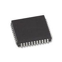
ST16C550IJ44-F Exar Corporation, ST16C550IJ44-F Datasheet - Page 11

ST16C550IJ44-F
Manufacturer Part Number
ST16C550IJ44-F
Description
IC UART FIFO 16B SGL 44PLCC
Manufacturer
Exar Corporation
Type
UART with 16-byte FIFOsr
Datasheet
1.ST16C550CJ44-F.pdf
(35 pages)
Specifications of ST16C550IJ44-F
Number Of Channels
1, UART
Package / Case
44-LCC (J-Lead)
Features
*
Fifo's
16 Byte
Voltage - Supply
2.97 V ~ 5.5 V
With False Start Bit Detection
Yes
With Modem Control
Yes
With Cmos
Yes
Mounting Type
Surface Mount
Data Rate
1.5 Mbps
Supply Voltage (max)
5.5 V
Supply Voltage (min)
2.97 V
Supply Current
3 mA
Maximum Operating Temperature
+ 85 C
Minimum Operating Temperature
- 40 C
Mounting Style
SMD/SMT
Operating Supply Voltage
3.3 V, 5 V
No. Of Channels
1
Supply Voltage Range
2.97V To 5.5V
Operating Temperature Range
-40°C To +85°C
Digital Ic Case Style
PLCC
No. Of Pins
44
Filter Terminals
SMD
Rohs Compliant
Yes
Lead Free Status / RoHS Status
Lead free / RoHS Compliant
Lead Free Status / RoHS Status
Lead free / RoHS Compliant, Lead free / RoHS Compliant
Other names
1016-1261
Available stocks
Company
Part Number
Manufacturer
Quantity
Price
Company:
Part Number:
ST16C550IJ44-F
Manufacturer:
Exar Corporation
Quantity:
135
Company:
Part Number:
ST16C550IJ44-F
Manufacturer:
Exar Corporation
Quantity:
10 000
Part Number:
ST16C550IJ44-F
Manufacturer:
EXAR/艾科嘉
Quantity:
20 000
DMA Operation
The ST16C550 FIFO trigger level provides additional
flexibility to the user for block mode operation. The user
can optionally operate the transmit and receive FIFO’s
in the DMA mode (FCR bit-3). The DMA mode affects
the state of the -RXRDY and -TXRDY output pins. The
following tables show this:
Loop-back Mode
The internal loop-back capability allows onboard diag-
nostics. In the loop-back mode the normal modem
interface pins are disconnected and reconfigured for
loop-back internally. In this mode MSR bits 4-7 are
also disconnected. However, MCR register bits 0-3
can be used for controlling loop-back diagnostic test-
ing. In the loop-back mode -OP1 and -OP2 in the MCR
register (bits 0-1) control the modem -RI and -CD
inputs respectively. MCR signals -DTR and -RTS (bits
0-1) are used to control the modem -CTS and -DSR
inputs respectively. The transmitter output (TX) and the
receiver input (RX) are disconnected from their associ-
ated interface pins, and instead are connected together
internally (See Figure 4). The -CTS, -DSR, -CD, and -RI
are disconnected from their normal modem control
inputs pins, and instead are connected internally to -
DTR, -RTS, -OP1 and -OP2. Loop-back test data is
entered into the transmit holding register via the user
data bus interface, D0-D7. The transmit UART serial-
izes the data and passes the serial data to the receive
UART via the internal loop-back connection. The receive
UART converts the serial data back into parallel data
that is then made available at the user data interface,
-RXRDY pin:
Non-DMA mode
1 = FIFO empty
0 = at least 1 byte
-TXRDY pin:
Non-DMA mode
1 = at least 1 byte
0 = FIFO empty
Rev. 5.01
in FIFO
in FIFO
DMA mode
0 to 1 transition when FIFO
empties
1 to 0 transition when FIFO
reaches trigger level, or
timeout occurs
DMA mode
1 = FIFO is full
0 = FIFO has at least 1
empty location
11
D0-D7. The user optionally compares the received
data to the initial transmitted data for verifying error
free operation of the UART TX/RX circuits.
In this mode , the receiver and transmitter interrupts are
fully operational. The Modem Control Interrupts are also
operational. The interrupts are still controlled by the
IER.
Figure 3, TYPICAL EXTERNAL CRYSTAL OSCIL-
LATOR CONNECTION
XTAL1
22-47pF
C1
Y1
R2
ST16C550
1M
XTAL2
1.8432 - 24 MHz
22-47pF
(Optional)
C2
R1
0-120


