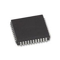
ST16C550IJ44-F Exar Corporation, ST16C550IJ44-F Datasheet - Page 4

ST16C550IJ44-F
Manufacturer Part Number
ST16C550IJ44-F
Description
IC UART FIFO 16B SGL 44PLCC
Manufacturer
Exar Corporation
Type
UART with 16-byte FIFOsr
Datasheet
1.ST16C550CJ44-F.pdf
(35 pages)
Specifications of ST16C550IJ44-F
Number Of Channels
1, UART
Package / Case
44-LCC (J-Lead)
Features
*
Fifo's
16 Byte
Voltage - Supply
2.97 V ~ 5.5 V
With False Start Bit Detection
Yes
With Modem Control
Yes
With Cmos
Yes
Mounting Type
Surface Mount
Data Rate
1.5 Mbps
Supply Voltage (max)
5.5 V
Supply Voltage (min)
2.97 V
Supply Current
3 mA
Maximum Operating Temperature
+ 85 C
Minimum Operating Temperature
- 40 C
Mounting Style
SMD/SMT
Operating Supply Voltage
3.3 V, 5 V
No. Of Channels
1
Supply Voltage Range
2.97V To 5.5V
Operating Temperature Range
-40°C To +85°C
Digital Ic Case Style
PLCC
No. Of Pins
44
Filter Terminals
SMD
Rohs Compliant
Yes
Lead Free Status / RoHS Status
Lead free / RoHS Compliant
Lead Free Status / RoHS Status
Lead free / RoHS Compliant, Lead free / RoHS Compliant
Other names
1016-1261
Available stocks
Company
Part Number
Manufacturer
Quantity
Price
Company:
Part Number:
ST16C550IJ44-F
Manufacturer:
Exar Corporation
Quantity:
135
Company:
Part Number:
ST16C550IJ44-F
Manufacturer:
Exar Corporation
Quantity:
10 000
Part Number:
ST16C550IJ44-F
Manufacturer:
EXAR/艾科嘉
Quantity:
20 000
ST16C550
SYMBOL DESCRIPTION
A0
A1
A2
IOR
CS0
CS1
IOW
-AS
D0-D7
GND
-CS2
Symbol
Rev. 5.01
1-8
40
28
27
26
22
12
13
14
19
25
20
Pin
2-9
44
31
30
29
25
14
15
16
21
28
22
43-47
2-4
28
48
27
26
20
10
11
17
24
18
9
Signal
type
Pwr
I/O
I
I
I
I
I
I
I
I
I
Address-0 Select Bit Internal registers address selection.
Address-1 Select Bit Internal registers address selection.
Address-2 Select Bit Internal registers address selection.
Read data strobe. Its function is the same as -IOR (see -
IOR), except it is active high. Either an active -IOR or IOR
is required to transfer data from 16C550 to CPU during a
read operation. Connect to logic 0 when using -IOR.
Chip Select-0. Logical 1 on this pin provides the chip select-
0 function. Connect CS0 to logic 1 if using CS1 or -CS2.
Chip Select-1. Logical 1 on this pin provides the chip select-
1 function. Connect CS1 to logic 1 if using CS0 or -CS2.
Chip Select -2. Logical 0 on this pin provides the chip select-
2 function. Connect to logic 0 if using CS0 or CS1.
Write data strobe. Its function is the same as -IOW (see -
IOW), but it acts as an active high input signal. Either -IOW
or IOW is required to transfer data from the CPU to
ST16C550 during a write operation. Connect to logic 0 when
using -IOW.
Address Strobe. A logic 1 transition on -AS latches the state
of the chip selects and the register select bits, A0-A2. This
input is used when address and chip selects are not stable
for the duration of a read or write operation, i.e., a micropro-
cessor that needs to de-multiplex the address and data bits.
If not required, the -AS input can be permanently tied to a
logic 0.
Data Bus (Bi-directional) - These pins are the eight bit, tri-
state data bus for transferring information to or from the
controlling CPU. D0 is the least significant bit and the first
data bit in a transmit or receive serial data stream.
Signal and Power Ground.
4
Pin Description


