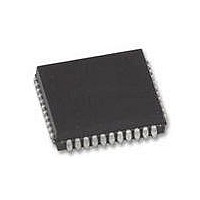
ST16C550IJ44-F Exar Corporation, ST16C550IJ44-F Datasheet - Page 6

ST16C550IJ44-F
Manufacturer Part Number
ST16C550IJ44-F
Description
IC UART FIFO 16B SGL 44PLCC
Manufacturer
Exar Corporation
Type
UART with 16-byte FIFOsr
Datasheet
1.ST16C550CJ44-F.pdf
(35 pages)
Specifications of ST16C550IJ44-F
Number Of Channels
1, UART
Package / Case
44-LCC (J-Lead)
Features
*
Fifo's
16 Byte
Voltage - Supply
2.97 V ~ 5.5 V
With False Start Bit Detection
Yes
With Modem Control
Yes
With Cmos
Yes
Mounting Type
Surface Mount
Data Rate
1.5 Mbps
Supply Voltage (max)
5.5 V
Supply Voltage (min)
2.97 V
Supply Current
3 mA
Maximum Operating Temperature
+ 85 C
Minimum Operating Temperature
- 40 C
Mounting Style
SMD/SMT
Operating Supply Voltage
3.3 V, 5 V
No. Of Channels
1
Supply Voltage Range
2.97V To 5.5V
Operating Temperature Range
-40°C To +85°C
Digital Ic Case Style
PLCC
No. Of Pins
44
Filter Terminals
SMD
Rohs Compliant
Yes
Lead Free Status / RoHS Status
Lead free / RoHS Compliant
Lead Free Status / RoHS Status
Lead free / RoHS Compliant, Lead free / RoHS Compliant
Other names
1016-1261
Available stocks
Company
Part Number
Manufacturer
Quantity
Price
Company:
Part Number:
ST16C550IJ44-F
Manufacturer:
Exar Corporation
Quantity:
135
Company:
Part Number:
ST16C550IJ44-F
Manufacturer:
Exar Corporation
Quantity:
10 000
Part Number:
ST16C550IJ44-F
Manufacturer:
EXAR/艾科嘉
Quantity:
20 000
ST16C550
SYMBOL DESCRIPTION
-DDIS
-OP1
RESET
RCLK
-OP2
VCC
XTAL1
XTAL2
-CD
Symbol
Rev. 5.01
40
23
34
35
31
40
16
17
38
9
Pin
26
39
44
38
10
35
44
18
19
42
48
22
34
35
31
14
15
5
42
40
Signal
type
Pwr
O
O
O
O
I
I
I
I
Drive Disable. This pin goes to a logic 0 when the external
CPU is reading data from the ST16C550. This signal can be
used to disable external transceivers or other logic func-
tions.
Output-1 (User Defined) - See bit-2 of modem control
register (MCR bit-2).
Reset. (active high) - A logic 1 on this pin will reset the
internal registers and all the outputs. The UART transmitter
output and the receiver input will be disabled during reset
time. (See ST16C550 External Reset Conditions for initial-
ization details.)
Receive Clock Input. This pin is used as external 16X clock
input to the receiver section. External connection to -
Baudout pin is required in order to utilize the internal baud
rate generator.
Output-2 (User Defined). This pin provides the user a
general purpose output. See bit-3 modem control register
(MCR bit-3).
Power Supply Input.
Crystal or External Clock Input - Functions as a crystal input
or as an external clock input. A crystal can be connected
between this pin and XTAL2 to form an internal oscillator
circuit. An external 1 M
XTAL1 and XTAL2 pins (see figure 3). Alternatively, an
external clock can be connected to this pin to provide
custom data rates (Programming Baud Rate Generator
section).
Output of the Crystal Oscillator or Buffered Clock - (See also
XTAL1). Crystal oscillator output or buffered clock output.
Carrier Detect (active low) - A logic 0 on this pin indicates
that a carrier has been detected by the modem.
6
Pin Description
resistor is required between the


