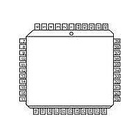
ST16C2552IJ44-F Exar Corporation, ST16C2552IJ44-F Datasheet - Page 8

ST16C2552IJ44-F
Manufacturer Part Number
ST16C2552IJ44-F
Description
IC UART FIFO 16B DUAL 44PLCC
Manufacturer
Exar Corporation
Type
RS- 232 or RS- 485r
Specifications of ST16C2552IJ44-F
Number Of Channels
2, DUART
Package / Case
44-LCC (J-Lead)
Features
*
Fifo's
16 Byte
Protocol
RS232, RS485
Voltage - Supply
3.3 V ~ 5 V
With False Start Bit Detection
Yes
With Modem Control
Yes
With Cmos
Yes
Mounting Type
Surface Mount
Data Rate
4 Mbps
Supply Voltage (max)
5.5 V
Supply Voltage (min)
2.97 V
Supply Current
3 mA
Maximum Operating Temperature
+ 85 C
Minimum Operating Temperature
- 40 C
Mounting Style
SMD/SMT
Operating Supply Voltage
3.3 V or 5 V
No. Of Channels
2
Supply Voltage Range
2.97V To 5.5V
Operating Temperature Range
-40°C To +85°C
Digital Ic Case Style
PLCC
No. Of Pins
44
Filter Terminals
SMD
Rohs Compliant
Yes
Lead Free Status / RoHS Status
Lead free / RoHS Compliant
Lead Free Status / RoHS Status
Lead free / RoHS Compliant, Lead free / RoHS Compliant
Other names
1016-1258-5
Available stocks
Company
Part Number
Manufacturer
Quantity
Price
Company:
Part Number:
ST16C2552IJ44-F
Manufacturer:
Exar Corporation
Quantity:
135
Company:
Part Number:
ST16C2552IJ44-F
Manufacturer:
IDT
Quantity:
4 795
Company:
Part Number:
ST16C2552IJ44-F
Manufacturer:
Exar Corporation
Quantity:
10 000
ST16C2552
2.97V TO 5.5V DUAL UART WITH 16-BYTE FIFO
Each UART channel in the 2552 has a set of enhanced registers for controlling, monitoring and data loading
and unloading. The configuration register set is compatible to those already available in the standard single
16C550 and dual ST16C2550. These registers function as data holding registers (THR/RHR), interrupt status
and control registers (ISR/IER), a FIFO control register (FCR), receive line status and control registers (LSR/
LCR), modem status and control registers (MSR/MCR), programmable data rate (clock) divisor registers (DLL/
DLM), and a user accessible scratchpad register (SPR).
Beyond the general 16C2550 features and capabilities, the 2552 offers the Alternate Function Register which
allows simultaneous writes to both channels. All the register functions are discussed in full detail later in
“Section 3.0, UART INTERNAL REGISTERS” on page
During a write mode cycle, the setting of Alternate Function Register (AFR) bit-0 to a logic 1 will override the
CHSEL selection and allows a simultaneous write to both UART channel sections. This functional capability
allow the registers in both UART channels to be modified concurrently, saving individual channel initialization
time. Caution should be exercised, however, when using this capability. Any in-process serial data transfer
may be disrupted by changing an active channel’s mode.
The device does not support direct memory access. The DMA Mode (a legacy term) in this document doesn’t
mean “direct memory access” but refers to data block transfer operation. The DMA mode affects the state of
the RXRDY# A/B (MF# A/B becomes RXRDY# A/B output when AFR[2:1] = ‘10’) and TXRDY# A/B output
pins. The transmit and receive FIFO trigger levels provide additional flexibility to the user for block mode
operation. The LSR bits 5-6 provide an indication when the transmitter is empty or has an empty location(s) for
more data. The user can optionally operate the transmit and receive FIFO in the DMA mode (FCR bit-3=1).
When the transmit and receive FIFO are enabled and the DMA mode is disabled (FCR bit-3 = 0), the 2552 is
placed in single-character mode for data transmit or receive operation. When DMA mode is enabled (FCR bit-
3 = 1), the user takes advantage of block mode operation by loading or unloading the FIFO in a block
sequence determined by the programmed trigger level. The following table show their behavior. Also see
Figures
2.4
2.5
2.6
RXRDY# A/B
TXRDY# A/B
P
INS
Channel A and B Internal Registers
Simultaneous Write to Channel A and B
DMA Mode
16
through 21.
0 = 1 byte.
1 = no data.
0 = THR empty.
1 = byte in THR.
(FIFO D
FCR
T
ABLE
BIT
ISABLED
-0=0
2: TXRDY#
)
0 = at least 1 byte in FIFO
1 = FIFO empty.
0 = FIFO empty.
1 = at least 1 byte in FIFO.
(DMA Mode Disabled)
AND
FCR Bit-3 = 0
RXRDY# O
8
UTPUTS IN
15.
FCR B
IT
-0=1 (FIFO E
FIFO
1 to 0 transition when FIFO reaches the trigger
level, or timeout occurs.
0 to 1 transition when FIFO empties.
0 = FIFO has at least 1 empty location.
1 = FIFO is full.
AND
DMA M
(DMA Mode Enabled)
NABLED
FCR Bit-3 = 1
ODE
)
REV. 4.2.2


